
Design Guide

System Memory Design Guidelines (DDR-SDRAM) for Memory Down Configuration
R
Intel
®
855GM/855GME Chipset Platform Design Guide 125
7.3.3. DDR Clock Routing Guidelines
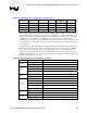
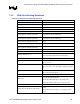
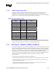
Table 44. Clock Signal Group Routing Guidelines
Parameter Definition
Signal Group SCK[5:0] and SCK#[5:0]
Topology Differential Pair Point to Point
Reference Plane Ground Referenced
Single Ended Trace Impedance ( Zo ) 42 ohms +/-15%
Differential Mode Impedance (Zdiff) 70 ohms +/- 15%
Nominal Trace Width
(see exceptions for breakout region below)
Inner Layers: 7 mils
Outer Layers: 8 mils (pin escapes only)
Nominal Pair Spacing (edge to edge)
(see exceptions for breakout region below)
Inner Layers: 4 mils
Outer Layers: 5 mils (pin escapes only)
Minimum Pair to Pair Spacing
(see exceptions for breakout region below)
20 mils
Minimum Serpentine Spacing 20 mils
Minimum Spacing to Other DDR Signals
(see exceptions for breakout region below)
20 mils
Minimum Isolation Spacing to non-DDR Signals 25 mils
Maximum Via Count 2 (per side Micro-Dimm) 5 (per side Memory Down)
Package Length Range – P1
1000 mils +/- 350mils
(See clock package length Table 45 for exact lengths.)
L1 Max = 300 mils (breakout segment)
L2
Min = 0.25 inches
Max = 4.5 inches
L3
Max = .5” inches (see Figure 54)
Min = 0.25 in. Max = 1.0 in. (See Figure 55, Figure 56 and Figure
57)
L4
Max = 0.5 inches (see Figure 55 and Figure 57)
Max = 0.25 inches (see Figure 56)
L5 Max = 0.25 inches
Total Length
Total length target is determined by placement (see Figure 54,
Figure 55, Figure 56 and Figure 57)
Total length for Micro-DIMM group = X0 (see Figure 58)
Total length for Memory Down group = X1 (see Figure 58)
SCK to SCK# Length Matching Match total length to +/- 10 mils (see Section 7.3.3.1)
Clock to Clock Length Matching (Total Length)
Match all Micro-DIMM clocks to X0 +/- 25 mils (see section
7.3.3.2)
Match all Memory Down clocks to X1 +/- 25 mils (see section
7.3.3.2)