
Design Guide

System Memory Design Guidelines (DDR-SDRAM) for Memory Down Configuration
R
126 Intel
®
855GM/855GME Chipset Platform Design Guide
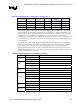
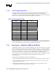
Parameter Definition
Breakout Exceptions
(Reduced geometries for GMCH breakout region)
Inner Layers: 4 mil trace, 4 mil pair space allowed
Outer Layers: 5 mil trace, 5 mil pair space allowed
Pair to pair spacing of 5 mils allowed
Spacing to other DDR signals of 5 mils allowed
Maximum breakout length is 0.3”
NOTES:
1. Pad to Pin length tuning is utilized on clocks in order to achieve minimal variance. Package lengths range
between approximately 600 mils and 1400 mils. Exact package lengths for each clock signal are provided at
the end of this Section. Overall target length should be established based on placement and routing flow. The
resulting motherboard segment lengths must fall within the ranges specified.
2. The DDR clocks should be routed on internal layers, except for pin escapes. It is recommended that pin escape
vias be located directly adjacent to the ball pads on all clocks. Surface layer routing should be minimized.
3. Exceptions to the trace width and spacing geometries are allowed in the breakout region in order to fanout the
interconnect pattern. Reduced spacing should be avoided as much as possible.
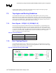
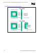
7.3.3.1. Clock Length Matching Requirements
The GMCH chipset provides two differential clock pairs for the Micro-DIMM and two pairs for
Memory Down. A differential clock pair is made up of a SCK signal and its complement signal SCK#.
Refer to Section 2.2 for more details on length matching requirements.
The differential pairs for the Micro-DIMM are:
SCK[0] / SCK#[0]
SCK[1] / SCK#[1]
The differential pairs for Memory Down are:
SCK[3] / SCK#[3]
SCK[4] / SCK#[4]
The SCK[2]/SCK#[2] and SCK[5]/SCK#[5] differential clock signals are not routed for this
configuration and should be left as no connects on the motherboard. These clocks are associated with
ECC. ECC is not supported by these routing guidelines.
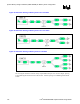
The two sets of differential clocks must be length tuned on the motherboard such that any pair to pair
package length variation is tuned out. The three pairs associated with Micro-DIMM are tuned to a fixed
overall length, including package, and the two pairs associated with Memory Down are tuned to a fixed
overall length.
The two traces associated with each clock pair are length matched within the package, however some
additional compensation may be required on the motherboard in order to achieve the ± 10 mil length
tolerance within the pair.
Between clock pairs the package length varies substantially. Therefore, the motherboard length of each
clock pair must be length adjusted to tune out package variance. The total length including package
should be matched to within ± 25 mils of each other, as shown in the
Length Range Formula for Micro-DIMM: