
Design Guide

System Memory Design Guidelines (DDR-SDRAM) for Memory Down Configuration
R
Intel
®
855GM/855GME Chipset Platform Design Guide 127
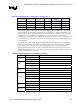
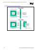
X0 = SCK/SCK#[1:0] P1 + L1 + L2 + L3 (see Figure 54)
Length Range Formulas for Memory Down
:
X1 = SCK/SCK#[4:3] P1 + L1 + L2 + L3 + L4 (see Figure 55)
= SCK/SCK#[4:3] P1 + L1 + L2 + L3 + L4 + L5 (see Figure 56 and Figure 57)
This may result in a clock length variance of as much as 700 mils on the motherboard.
The first step in determining the routing lengths for clocks and all other clock relative signal groups is to
establish the target length for each clock group. These target lengths are shown as X0 and X1, in
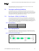
Length Range Formula for Micro-DIMM:
X0 = SCK/SCK#[1:0] P1 + L1 + L2 + L3 (see Figure 54)
Length Range Formulas for Memory Down
:
X1 = SCK/SCK#[4:3] P1 + L1 + L2 + L3 + L4 (see Figure 55)
= SCK/SCK#[4:3] P1 + L1 + L2 + L3 + L4 + L5 (see Figure 56 and Figure 57)
These are the lengths to which all clocks within the corresponding group will be matched, and the
reference length values used to calculate the length ranges for the other signal groups.
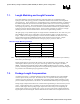
7.3.3.2. Clock Reference Lengths
The clock reference length for each Micro-DIMM and Memory Down clock group is determined by first
determining the longest total clock length required to complete the clock routing. A table of clock
package lengths is provided in Table 45 to assist in this calculation. Once the longest total length is
determined for each clock group, this becomes a lower bound for the associated clock reference length.
At this point it is helpful to have completed a test route of the SDQ/SDQS bus such that final clock
reference lengths can be defined with consideration of the impact on SDQ/SDQS bus routability. Some
iteration may be required.
Once the reference lengths X0 and X1 are defined then the next step is to tune each clock pair's
motherboard trace segment lengths as required such that the overall length of each clock equals the
associated clock reference length plus or minus the 25 mil tolerance. Again, the reference length for the
two sets of clocks should be offset by the nominal routing length between the Micro-DIMM connector
pad and Memory Down Device Pin.
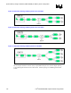
Length Range Formula for Micro-DIMM:
X0 = SCK/SCK#[1:0] P1 + L1 + L2 + L3 (see Figure 54)
Length Range Formulas for Memory Down
:
X1 = SCK/SCK#[4:3] P1 + L1 + L2 + L3 + L4 (see Figure 55)
= SCK/SCK#[4:3] P1 + L1 + L2 + L3 + L4 + L5 (see Figure 56 and Figure 57)