
Design Guide

System Memory Design Guidelines (DDR-SDRAM) for Memory Down Configuration
R
Intel
®
855GM/855GME Chipset Platform Design Guide 129
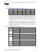
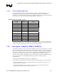
7.3.3.3. Clock Package Length Table
The package length data in the table below should be used to tune the motherboard length of each
SCK/SCK# clock pair between the GMCH and the Micro-DIMM connector or memory down
component. It is recommended that die-pad to Micro-DIMM or memory down component pad length be
tuned to within ± 25 mils in order to optimize timing margins on the interface.
Table 45. DDR Clock Package Lengths
Signal Pin Number
Package Length
(mils)
SCLK_0 AB2 1177
SCLK#_0 AA2 1169
SCLK_1 AC26 840
SCLK#_1 AB25 838
SCLK_2 AC3 1129
SCLK#_2 AD4 1107
SCLK_3 AC2 1299
SCLK#_3 AD2 1305
SCLK_4 AB23 643
SCLK#_4 AB24 656
SCLK_5 AA3 1128
SCLK#_5 AB4 1146
Package length compensation can be performed on each individual clock output thereby matching total
length on SCK/SCK# exactly, or alternatively the average package length can be used for both outputs
of a pair and length tuning done with respect to the motherboard portion only.
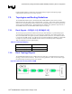
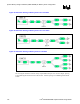
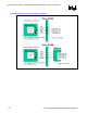
7.3.4. Data Signals – SDQ[63:0], SDM[7:0], SDQS[7:0]
The GMCH data signals are source synchronous signals that include a 72-bit wide data bus, 8 check bits
for Error Checking and Correction (ECC), a set of 9 Data Mask bits, and a set of 9 data strobe signals.
There is an associated data strobe and data mask bit for each of the 8-bit data byte groups, making for a
total of nine – 10-bit byte lanes. ECC is a feature not supported by Micro-DIMMs and will therefore not
be supported by the memory down topology. It is recommended that these signals be left as no
connects. Further reference to data signals reserved for ECC will not be made in this RDDP addendum.
This section summarizes the SDQ/SDM to SDQS routing guidelines and length matching
recommendations.
The data signals include SDQ [63:0], SDM[7:0], and SDQS[7:0].
• The data signals should transition from an external layer to an internal signal layer under the GMCH.
• At the Micro-DIMM connector, the signal should transition to an external layer and connect to the
appropriate pad on the connector.
• After the Micro-DIMM transition, continue to route the signal on the same internal layer until
transitioning back to an external layer at the series resistor.