
Design Guide

System Memory Design Guidelines (DDR-SDRAM) for Memory Down Configuration
R
130 Intel
®
855GM/855GME Chipset Platform Design Guide
• After the series resistor, the signal should transition from the external layer to the same internal layer
and route to the SDRAM device.
• Transition back out to an external layer and connect to the appropriate SDRAM pad.
• Connection to the termination resistor should be via the same internal layer with a transition back to
the external layer near the resistor. External trace lengths should be minimized.
To facilitate routing, swapping of the byte lanes is allowed for SDQ[63:0] only. Bit swapping within the
byte lane is also allowed for SDQ[63:0] only. All internal and external signals should be ground
sandwiched to keep the path of the return current continuous.
Resistor packs are acceptable for the series (Rs) and parallel (Rt) data and strobe termination resistors,
but data and strobe signals cannot be placed within the same R pack as the command or control signals.
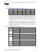
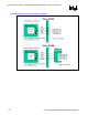
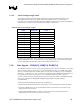
The table and diagrams below depict the recommended topology and layout routing guidelines for the
DDR-SDRAM data signals.
Intel recommends that the full data bus SDQ[63:0], mask bus SDM[7:0], and strobe signals SDQS[7:0]
be routed on the same internal signal layer. It is required that the SDQ byte group and the associated
SDM and SDQS signals within a byte lane be routed on the same internal layer.
The total length of SDQ, SDM, and SDQS traces between the GMCH and the Micro-DIMM/Memory
Down devices must be within the range defined in the overall guidelines, and is also constrained by a
length range boundary based on SCK/SCK# clock length, and a SDQ/SDM to SDQS length matching
requirement within each byte lane. Note also that all length matching must be done inclusive of package
length. A table of SDQ, SDM, and SDQS package lengths is provided at the end of this Section to
facilitate this process.
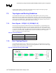
There are two levels of matching implemented on the data bus signals.
• The first is the length range constraint on the SDQS signals based on clock reference length.
• The second is SDQ/SDM to SDQS length matching within a byte lane.
The length of the SDQS signal for each byte lane must fall within a range determined by the clock
reference length, as defined in the SDQS to SCK/SCK# length matching section. The actual length of
SDQS for each byte lane may fall anywhere within this range based on placement and routing flow.
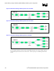
Once the SDQS length for a byte lane is established, the SDQ, SDM, and SDQS signals within the byte
lane must be length matched to each other, inclusive of package length, as described in the SDQ to
SDQS length matching section.