
Design Guide


System Memory Design Guidelines (DDR-SDRAM) for Memory Down Configuration
R
132 Intel
®
855GM/855GME Chipset Platform Design Guide
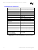
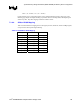
Table 46. Data Signal Group Routing Guidelines
Parameter Definition
Signal Group SDQ[63:0], SDQS[7:0], SDM[7:0]
Motherboard Topology Daisy Chain with Parallel Termination
Reference Plane Ground sandwiching required
Characteristic Trace Impedance (Zo) 55 Ω +/- 15%
Parallel Termination Resistor (Rt) 56 Ω +/- 5%
Series Resistor (Rs) 33 Ω +/- 5%
Nominal Trace Width
Inner layers: 4 mils
Outer layers: 5 mils
Minimum Spacing to Trace Width Ratio
SDQ/SDM: 2 to 1 (e.g. 8 mil space to 4 mil trace)
SDQS: 3 to 1 (e.g. 12 mil space to 4 mil space)
Minimum Isolation Spacing to non-DDR Signals 20 mils
Package Length P1
700 mils +/- 300 mils
(see package length Table 48 for exact lengths.)
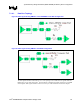
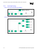
Stub Length S1 Max = 0.10 inches
L1
Min = 0.25 inches (See Figure 59 and Figure 60)
Max = 2.5 inches
L2 Max = 0.75 inches (See Figure 59 and Figure 60)
L3 Max = 1.25 inches (See Figure 59 and Figure 60)
L4 Max = 0.25 inches(See Figure 59 and Figure 60)
L5 Max = 1.25 inches (See Figure 59 and Figure 60)
L6 Max = 0.05 inches (See Figure 60)
Max Length:
L1+L2+L3+L4+L5 (see Figure 59)
L1+L2+L3+L4+L5+L6 (see Figure 60)
Max = 4.25 inches
NOTES:
1. Power distribution vias from Rt to Vtt are not included in this count.
2. The overall minimum and maximum length to the Micro-DIMM and Memory Down must comply with clock length
matching requirements.