
Design Guide


System Memory Design Guidelines (DDR-SDRAM) for Memory Down Configuration
R
Intel
®
855GM/855GME Chipset Platform Design Guide 133
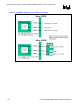
7.3.4.2. SDQS to Clock Length Matching Requirements
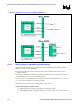
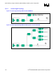
The first step in length matching is to determine the SDQS length range based on the SCK/SCK#
reference length defined previously. The total length of the SDQS strobe signals, including package
length, between the GMCH die-pad and the Micro-DIMM/Memory Down device must fall within the
range defined in the formulas below. See the clock Section for the definition of the clock reference
length. Refer to Figure 59 and Figure 60 for the definition of the various trace segments. The length
tuning requirements are also depicted in Figure 62. Refer to Section 7.1 for more details on length
matching and length formula requirements.
Length range formula for Micro-DIMM:
X
0
= SCK/SCK#[1:0] total reference length, including package length
Y
0
= SDQS[7:0] total length = GMCH package(P1) + L1 + S1, see Figure 59 and Figure 60,
where: ( X
0
– 2.0” ) ≤ Y
0
≤ ( X
0
+ 0.5” )
Length range formulas for Memory Down,
X
1
= SCK/SCK#[4:3] total reference length, including package length
Y
1
= SDQS[7:0] total length = GMCH package(P1) + L1 + L2 + L4 + L5, see Figure 59,
= SDQS[7:0] total length = GMCH package(P1) + L1 + L2 + L4 + L5 + L6, see Figure 60,
where: ( X
1
– 2.0” ) ≤ Y
1
≤ ( X
1
+ 0.5” )
Length matching is only performed from the GMCH to the Micro-DIMM or memory down devices, and
does not involve the length of L3, which can vary over its entire range. Note that a nominal SDQS
package length of 750 mils can be used to estimate motherboard lengths prior to performing package
length compensation. Refer to Section 7.2 for more details on package length compensation.