
Design Guide


System Memory Design Guidelines (DDR-SDRAM) for Memory Down Configuration
R
134 Intel
®
855GM/855GME Chipset Platform Design Guide
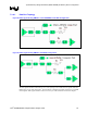
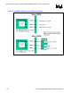
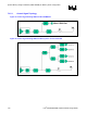
Figure 61. SDQS to Clock Trace Length Matching Diagram
7.3.4.3. Data to Strobe Length Matching Requirements
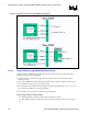
The data bit signals, SDQ[63:0] are grouped by byte lanes and associated with a data mask signal
SDM[8:0], and a data strobe, SDQS[8:0].
• The data and mask signals must be length matched to their associated strobe within ± 25 mils,
including package.
• For the Micro-DIMM this length matching includes the motherboard trace length to the pads of the
Micro-DIMM connector (L1+S1) plus package length.
• For Memory Down, the motherboard trace length to the pads of the SDRAM device (L1 + L2 + L4 +
L5 + L6 for the 2x16 BGA case) plus package length.
Refer to Section 0 for more details on package length compensation.
Length range formula for SDQ and SDM,
X = SDQS total length, including package length, as defined previously
Y = SDQ, SDM total length, including package length, within same byte lane as shown in Figure
62,