
Design Guide


System Memory Design Guidelines (DDR-SDRAM) for Memory Down Configuration
R
Intel
®
855GM/855GME Chipset Platform Design Guide 135
where: ( X – 25 mils ) ≤ Y ≤ ( X + 25 mils )
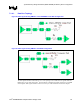
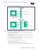
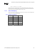
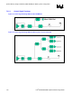
Length matching is not required for length L3 to the parallel termination resistors. Figure 62 on the
following page depicts the length matching requirements between the SDQ, SDM, and SDQS signals
within a byte lane. Byte lane mapping is defined in Table 47 below.
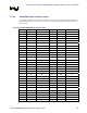
7.3.4.4. SDQ to SDQS Mapping
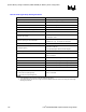
Table 47 below defines the mapping between the eight byte lanes, 8mask bits, and the 8 SDQS signals,
as required to do the required length matching.
Table 47. SDQ/SDM to SDQS Mapping
Signal Mask Relative To
SDQ[7:0] SDM[0] SDQS[0]
SDQ[15:8] SDM[1] SDQS[1]
SDQ[23:16] SDM[2] SDQS[2]
SDQ[31:24] SDM[3] SDQS[3]
SDQ[39:32] SDM[4] SDQS[4]
SDQ[56:40] SDM[5] SDQS[5]
SDQ[55:48] SDM[6] SDQS[6]
SDQ[63:56] SDM[7] SDQS[7]