
Design Guide


System Memory Design Guidelines (DDR-SDRAM) for Memory Down Configuration
R
138 Intel
®
855GM/855GME Chipset Platform Design Guide
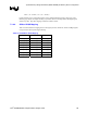
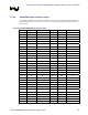
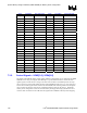
Signal Pin Number Pkg Length (mils) Signal Pin Number Pkg Length (mils)
SDQ_27 AF14 655 SDQ_59 AF28 756
SDQ_28 AG11 599 SDQ_60 AG26 782
SDQ_29 AD12 460 SDQ_61 AF26 748
SDQ_30 AF13 536 SDQ_62 AE27 673
SDQ_31 AH13 642 SDQ_63 AD27 608
SDQ_64 AG14 566 SDQS_0 AG2 925
SDQ_65 AE14 477 SDQS_1 AH5 838
SDQ_66 AE17 571 SDQS_2 AH8 756
SDQ_67 AG16 530 SDQS_3 AE12 466
SDQ_68 AH14 701 SDQS_4 AH17 678
SDQ_69 AE15 421 SDQS_5 AE21 487
SDQ_70 AF16 491 SDQS_6 AH24 770
SDQ_71 AF17 530 SDQS_7 AH27 858
SDQS_8 AD15 418
SDM_0 AE5 838
SDM_1 AE6 693
SDM_2 AE9 538
SDM_3 AH12 606
SDM_4 AD19 492
SDM_5 AD21 470
SDM_6 AD24 557
SDM_7 AH28 917
SDM_8 AH15 685
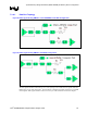
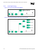
7.3.5. Control Signals – SCKE[3:0], SCS#[3:0]
The Montara-GM GMCH chipset control signals, SCKE[3:0] and SCS#[3:0], are clocked into the DDR
SDRAM devices using clock signals SCK/SCK#[4,3,1,0]. The GMCH drives the control and clock
signals together, with the clocks crossing in the valid control window. The GMCH provides one chip
select (CS) and one clock enable (CKE) signal per Micro-DIMM physical device row. Two chip select
and two clock enable signals will be routed to the Miro-DIMM. The remaining SCKE and CS# signals
can be routed to the memory down device configuration that the developer has chosen. Should the
memory down configuration contain one bank of memory SCKE[3] and SCS#[3] should be left as no
connects. Refer to Table 49 for the CKE and CS# signal to Micro-DIMM or Memory Down mapping.