
Design Guide


System Memory Design Guidelines (DDR-SDRAM) for Memory Down Configuration
R
Intel
®
855GM/855GME Chipset Platform Design Guide 139
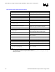
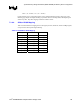
Table 49. Control Signal to Micro-DIMM/Memory Down Mapping
Signal Relative To SOPin
SCS#[0] Micro-DIMM Micro-DIMM Pin 95
SCS#[1] Micro-DIMM Micro-DIMM Pin 96
SCS#[2] Mem Down – Bank 1 Mem Device CS#
SCS#[3] Mem Down – Bank 2 Mem Device CS#
SCKE[0] Micro-DIMM Micro-DIMM Pin 72
SCKE[1] Micro-DIMM Micro-DIMM Pin 71
SCKE[2] Mem Down – Bank 1 Mem Device CKE#
SCKE[3] Mem Down – Bank 2 Mem Device CKE#
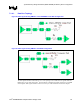
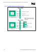
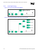
The following is an example layout description based on layout studies on an 8-layer board. The
Control signals should transition from an external layer to an internal signal layer (L1) under the
GMCH. If the signal is going to the Micro-DIMM connector, route the signal on the internal layer and
via to the external layer and connect to the appropriate pad on the connector (S1). If the signal is going
to the SDRAMs, route the signal on the internal layer until transitioning back to an external layer at the
parallel termination (L2). When it is close to the SDRAMs, the signal should via to another internal
layer and split into two traces (TL0). Each trace routes to the middle region of the SDRAM (TL1) and
via to the external layer. Depending on the number of devices for memory down, the Control signal can
be routed on the surface (TL2) to the ball or pad of one SDRAM or two SDRAMs. If 8 BGAs, the
signal will continue on from the via on an internal layer (TL2 on 8 BGA devices topology) and go to the
center region of the outer-most SDRAM then via to the external layer. Depending on the number of
devices for memory down, the Control signal can be routed on the surface (TL3 on 8 BGA devices
topology) to the ball or pad of one SDRAM device (4 TSOP SDRAMs) or two SDRAMs (8 BGAs).
External trace lengths should be minimized. All internal and external signals should be ground reference
to keep the path of return current continuous. Intel suggests that all control signals be routed on the same
internal layer.
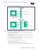
Resistor packs are acceptable for the parallel (Rt) control termination resistors, but control signals can’t
be placed within the same R pack as the data or command signals. Figure 62, Figure 63, Figure 64, &
Figure 65 and Table 50 below depicts the recommended topology and layout routing guidelines for the
DDR-SDRAM control signals.