
Design Guide


System Memory Design Guidelines (DDR-SDRAM) for Memory Down Configuration
R
Intel
®
855GM/855GME Chipset Platform Design Guide 143
7.3.5.3. Control to Clock Length Matching Requirements
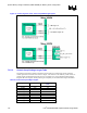
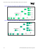
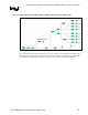
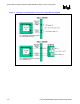
The length of the control signals, between the GMCH die pad and the Micro-DIMM/Memory Down
device must fall within the range defined below, with respect to the associated clock reference length. .
Refer to Figure 63, Figure 64, Figure 65, and Figure 66 for a definition of the various trace segments
that make up this path. The length of trace from the Micro-DIMM to the termination resistor need not
be length matched. The length matching requirements are also depicted in Figure 67. Refer to Section
Note: for more details on length matching requirements.
Length range formula for Micro-DIMM:
X
0
= SCK/SCLK#[1:0] total reference length, including package length. See clock Section 7.3.1.
Y
0
= SCS#[1:0] & SCKE[1:0] total length = P1 + L1+ S1, as shown in Figure 63.
where: ( X
0
– 2.0” ) ≤ Y
0
≤ ( X
0
- 0.5” )
Length range formula for Memory-Down:
X
1
= SCK/SCLK#[4:3] total reference length, including package length. See clock Section 7.3.1.
Y
1
= SCS#[3:2] & SCKE[3:2] total length = P1+L1+TL0+TL1+TL2 , as shown in Figure 64
= SCS#[3:2] & SCKE[3:2] total length = P1+L1+TL0+TL1+TL2+TL3, as shown in Figure 65
= SCS#[3:2] & SCKE[3:2] total length = P1+L1+TL0+TL1+ TL3, as shown in Figure 65
= SCS#[3:2] & SCKE[3:2] total length = P1+L1+TL0+TL1+TL2+TL3+TL4, as shown in
Figure 66
= SCS#[3:2] & SCKE[3:2] total length = P1+L1+TL0+TL1+TL3+TL4, as shown in Figure 66,
where: ( X
1
– 1.0” ) ≤ Y
1
≤ ( X
1
+ 0.5” )
No length matching is required to the termination resistor. Figure 67 on the following page depicts the
length matching requirements between the control signals and clock. A nominal CS/CKE package
length of 500 mils can be used to estimate baseline MB lengths. Refer to Section Note: for more details
on package length compensation.