
Design Guide


System Memory Design Guidelines (DDR-SDRAM) for Memory Down Configuration
R
144 Intel
®
855GM/855GME Chipset Platform Design Guide
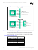
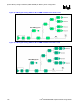
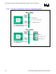
Figure 67. Control Signal to Clock Trace Length Matching Diagram
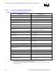
7.3.5.4. Control Group Package Length Table
The package length data in Table 51 should be used to match the overall length of each command
control signal to its associated clock reference length. Note that due to the relatively small variance in
package length and adequate timing margins it is acceptable to use a fixed 500-mil nominal package
length for all control signals, thereby reducing the complexity of the motherboard length calculations.
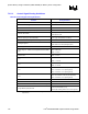
Table 51. Control Group Package Lengths
Signal Pin Number
Package Length
(mils)
SCS#[0] AD23 502
SCS#[1] AD26 659
SCS#[2] AC22 544
SCS#[3] AC25 612
SCKE[0] AC7 443
SCKE[1] AB7 389
SCKE[2] AC9 386
SCKE[3] AC10 376