
Design Guide


System Memory Design Guidelines (DDR-SDRAM) for Memory Down Configuration
R
Intel
®
855GM/855GME Chipset Platform Design Guide 149
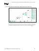
7.3.6.3. Command Topology Length Matching Requirements
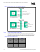
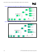
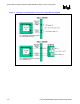
The routing length of the command signals between the GMCH die pad and Micro-DIMM/Memory
Down must be within the range defined below. This is with respect to the associated clock reference
length. Refer to Figure 43 for a definition of the various motherboard trace segments. The length of
trace from the Micro-DIMM to the termination resistor need not be length matched. The length
matching requirements are also depicted in Figure 71 Refer to Section 7.1 for more details on length
matching requirements.
Length range formula for Micro-DIMM:
X0 = SCK/SCLK#[1:0] total reference length, including package length (P1). See clock Section
7.3.1.
Y0 = CMD signal total length = P1 + L1+ S1, as shown in Figure 68, Figure 69, and Figure 70
where: ( X
0
– 2.0” ) ≤ Y
0
≤ ( X
0
+ 2.0” )
Length range formula for Memory-Down:
X1 = SCK/SCLK#[4:3] total reference length, including package length (P1). See clock section
7.3.1.
Y1 = CMD signal total length = P1 + L1 + L2 + TL0 + TL1 + TL2, as shown in Figure 68
= CMD signal total length = P1 + L1 + L2 + TL0 + TL1 + TL3 +TL4, as shown in Figure 69 &
Figure 70
= CMD signal total length = P1 + L1 + L2 + TL0 + TL1 + TL4, as shown in Figure 69 & Figure
70
= CMD signal total length = P1 + L1 + L2 + TL0 + TL2 + TL4, as shown in Figure 69 & Figure
70
= CMD signal total length = P1 + L1 + L2 + TL0 + TL2 + TL3 + TL4, as shown in Figure 69 &
Figure 70 where: ( X
1
– 2.0” ) ≤ Y
1
≤ ( X
1
+ 2.0” )
No length matching is required from Rs to the termination resistor. Figure 71 on the following page
depicts the length matching requirements between the command signals and clock. A nominal CMD
package length of 500 mils can be used to estimate baseline MB lengths. Refer to Note: for more details
on package length compensation.