
Design Guide

System Memory Design Guidelines (DDR-SDRAM) for Memory Down Configuration
R
Intel
®
855GM/855GME Chipset Platform Design Guide 155
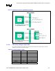
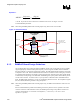
7.3.7.2. CPC Signal Routing Guidelines
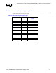
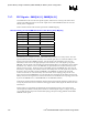
Table 55. CPC Signal Routing Guidelines
Parameter Routing Guidelines
Signal Group SMA[5,4,2,1], SMAB[5,4,2,1]
Motherboard Topology Point-to-Point with Parallel Termination
Reference Plane Ground Referenced
Characteristic Trace Impedance (Zo) 55 Ω ±15%
Nominal Trace Width
Inner layers: 4 mils
Outer layers: 5 mils
Minimum Spacing to Trace Width Ratio 2 to 1 (e.g. 8 mil space to 4 mil trace)
Minimum Isolation Spacing to non-DDR Signals 20 mils
Package Length P1
500 mils +/- 250 mils
(see Table 56 for exact package lengths.)
Trace Length S1 – Stub Length to Micro-DIMM
Connector
Max = 0.25”
Trace Length L1 – GMCH Control Signal Ball to
Micro-DIMM Pad
Min = 0.25 inches
Max = 4.0 inches
Trace Length L2 – Micro-DIMM Pad to Parallel
Termination Resistor Pad
Max = 2.0 inches
Trace Length TL0
Min = 0.25 inches
Max = 1.5 inches
Trace Length TL1
Min = 0.3 inches
Max = 0.7 inches
Trace Length TL2
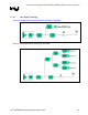
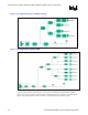
Min = 0.3 in Max = 0.7 in (see Figure 74 and Figure 75)
Min = 0.1 in Max = 0.5 in (see Figure 73)
Trace Length TL3
Min = 0.1 inches
Max = 0.5 inches
Parallel Termination Resistor (Rt) 56 Ω ± 5%
Maximum Recommended Motherboard Via
Count Per Signal
14
Length Matching Requirements
CPC to SCK/SCK# [5:0]
See length matching Section 7.3.7.3 and Figure 76 for details.
NOTES:
1. Variance per topology for TL1, TL2, and TL3 +
10 mils.