
Design Guide

Integrated Graphics Display Port
R
162 Intel
®
855GM/855GME Chipset Platform Design Guide
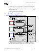
The analog switch should exhibit a low “on” resistance (< 8 Ω) and low parasitic capacitance (<10 pF).
The output routing from the analog switch should be routed as single-ended, 37.5-Ω impedance to the
75-Ω termination resistors that are located near the VGA connector on the motherboard and the VGA
connector on the docking station. The single-ended routing after these 75-Ω termination resistors to the
pi-filter and then to the VGA connector should be ideally 75-Ω. The recommended routing of the
termination resistors is shown in Figure 79.
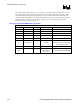
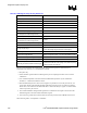
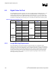
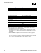
Table 57. Recommended GMCH DAC Components
Recommended DAC Board Components
Component Value Tolerance Power Type
R1 75.0 Ω 1% 1/16 W SMT, Metal Film
Refset
1
127.0 Ω 1% 1/16 W SMT, Metal Film
C1 0.1 uF 20% ----- SMT, Ceramic
C2 0.01 uF 20% ----- SMT, Ceramic
C 3.3 pF 10% ----- SMT, Ceramic
D
PAC DN006
-------
350 mW
California Micro Devices –
ESD diodes for VGA, SOIC package
Or equivalent diode array
FB 75 Ω @ 100 MHz -------- ------- MuRata* BLM11B750S
Analog
Switch
------- ------- Rated for a continuous
channel current of
100mA (min)
Ron < 8 Ω, Con < 10 pF
Texas Instruments SN74CB3Q3306
NOTE: Not needed when using 855GME platform with external graphics only.