
Design Guide

Integrated Graphics Display Port
R
Intel
®
855GM/855GME Chipset Platform Design Guide 163
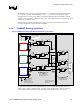
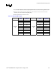
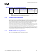
Figure 79. DAC R, G, B Routing and Resistor Layout example
Complement Output
(e.g. BLUE#)
DAC Output
(e.g. BLUE)
Via to
ground
plane
37.5
Ω
Trace Impedance
20 mil Space between channels
Intel 855GM
Chipset
Large via or multiple vias straight down to ground plane
No toggling signals sh
o
75.0Ω, 1%, 1/16W,
75.0
ANALOG
SWITC
H
37.5Ω Trace Impedance
VGA
Π-Filter
20 mil Space between channels
75Ω Trace Impedance
75.0
Ω
, 1%, 1/16W, SMT metal film resistor
75.0
VGA
Π-Filter
75Ω Trace Impedance
Termination Resistor placed on Dock Station
Near VGA connector
Termination Resistor placed on Motherboard
Near VGA connector
No toggling signals should be routed near these video outputs
Large via or multiple vias straight down to ground plane
NOTE: The routing to the docking connector is not shown in this figure; however, this routing scheme applies to the
docking connector as well.
8.1.5. DAC Power Requirements
The DAC requires a 1.5-V supply through its two VCCADAC balls. The two may share a set of
capacitors, 0.1 µF and 0.01 µF, but this connection should have low inductance. Separate analog power
or ground planes are not required for the DAC.
However, since the DAC is an analog circuit, it is particularly sensitive to AC noise seen on its power
rail. Designs should provide as clean and quiet a supply as possible to the VCCA_DAC. Additional
filtering and/or separate voltage rail may be needed to do so. On the Intel CRB, there is a placeholder
for a LC filter in case there is noise present in the VCCA power rail.
Video DAC Power Supply DC Specification: 1.50 V ± 5%
Video DAC Power Supply AC Specification:
+/- 0.3% from 0.10 Hz to 10 MHz
+/- 0.95% from 10 MHz to max pixel clock frequency
Absolute minimum voltage at the VCCA package ball = 1.40 V
Please refer to the latest Intel 855GM/GME (Montara-GM/GM+) Chipset GMCH EDS Addendum for
AC/CD specification.