
Design Guide

Integrated Graphics Display Port
R
Intel
®
855GM/855GME Chipset Platform Design Guide 165
kept minimal. LIBG pin is a current reference on the LVDS interface. A 1.5-kΩ pulldown is required
unless 855GME platform is being used with external graphics only option.
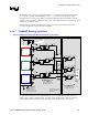
The following differential signal groups comprise the LVDS Interface. The topology rules for each
group are defined in subsequent sections.
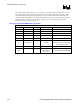
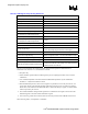
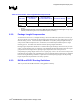
Table 58. Signal Group and Signal Pair Names
Channel Signal Group Signal Pair Names
Clocks ICLKAM, ICLKAP Channel A
Data Bus IYAM[3:0], IYAP[3:0]
Clocks ICLKBM, ICLKBP Channel B
Data Bus IYBM[3:0], IYBP[3:0]
8.2.1. LVDS Length Matching Constraints
The routing guidelines presented in the following subsections define the recommended routing
topologies, trace width and spacing geometries, and absolute minimum and maximum routed lengths for
each signal group. These recommendations are provided to achieve optimal SI and timing. In addition
to the absolute length limits provided, more restrictive length matching requirements are also provided.
The additional requirements further restrict the minimum to maximum length range of each signal group
with respect to clock strobe, as required to guarantee adequate timing margins.
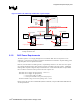
8.2.2. LVDS Package Length Compensation
As mentioned in Section 8.2.1, all length matching is done from GMCH die-pad to LVDS connector
pin. The reason for this is to compensate for the package length variation across each signal group in
order to minimize timing variance. The 855GM chipset GMCH does not equalize package lengths
internally as some previous GMCH components have, and therefore, the 855GM chipset GMCH
requires a length matching process. See Table 60 for the GMCH LVDS package lengths information.
Package length compensation should not be confused with length matching as discussed in the previous
section. Length matching refers to constraints on the minimum and maximum length bounds of a signal
group based on clock length, whereas package length compensation refers to the process of
compensating for package length variance across a signal group. There is of course some overlap in that
both affect the target length of an individual signal. Intel recommends that the initial route be completed
based on the length matching formulas in conjunction with nominal package lengths and that package
length compensation be performed as secondary operation.
8.2.3. LVDS Routing Guidelines
Each LVDS channel is required to be length matched to within ± 20 mils of the LVDS clock strobe
signals. The two complementary signals in each clock strobe pair, as well as in each data pair, are also
required to be length matched to within ± 20 mils of each other. See Table 59 for summary of LVDS
signal group routing guidelines.