
Design Guide

Integrated Graphics Display Port
R
170 Intel
®
855GM/855GME Chipset Platform Design Guide
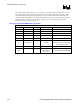
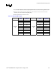
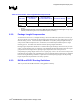
Table 63. DVOB and DVOC Routing Guideline Summary
Parameter Definition
Signal Group DVOBD [11:0], DVCBD [11:0]
Motherboard Topology Point to point
Reference Plane Ground Referenced
Characteristic Trace Impedance (Zo) 55 Ω ±15%
Nominal Trace Width Inner layers: 4 mils
Minimum Spacing to Trace Width Ratio 2 to 1 (e.g. 8 mil space to 4 mil trace)
Minimum Isolation Spacing to non-DVO Signals 20 mils
Minimum Spacing to Other DVO Signals 12 mils (see exceptions for breakout region below)
Minimum Spacing of DVOBCLK [1:0] or DVOCCLK [1:0]
to any other signals
12 mils
Package Length Range
See Table 64. DVO Interface Package Lengths for package
lengths.
Total Length
Min 1.5”
Max 6”
Data to Clock Strobe Length Matching Requirements ± 100 mils
CLK0 to CLK1 Length Matching Requirements ± 10 mils
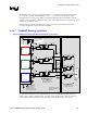
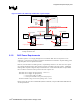
The DVO interface does not require external termination. They are routed point to point as follows:
• All signals should be routed as striplines (inner layers).
• All signals in a signal group should be routed on the same layer. Routing studies have shown that
these guidelines can be met. The trace length and trace spacing requirements must not be violated
by any signal.
• Route the DVOBCLK[1:0] or DVOCCLK[1:0] signal pairs 4 mils wide and 8 mils apart with a
max trace length of 6in. This signal pair should be a minimum of 12 mils from any adjacent
signals.
• In order to break out of the GMCH, the DVOB and/or DVOC data signals can be routed with a
trace width of 4 mils and a trace spacing of 7 mils. The signals should be separated to a trace width
of 4 mils and a trace spacing of 8 mils within 0.3 inches of the GMCH component.