
Design Guide

Integrated Graphics Display Port
R
Intel
®
855GM/855GME Chipset Platform Design Guide 171
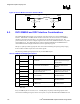
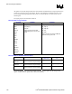
Table 64. DVO Interface Package Lengths
Signal
Pin
Number
Package Length
(mils)
Signal
Pin
Number
Package
Length (mils)
DVOBCLK P3 475 DVOCCLK J3 601
DVOBCLK# P4 439 DVOCCLK# J2 675
DVOBD[0] R3 489 DVOCD[0] K5 489
DVOBD[1] R5 439 DVOCD[1] K1 692
DVOBD[2] R6 343 DVOCD[2] K3 622
DVOBD[3] R4 415 DVOCD[3] K2 685
DVOBD[4] P6 409 DVOCD[4] J6 536
DVOBD[5] P5 387 DVOCD[5] J5 518
DVOBD[6] N5 466 DVOCD[6] H2 720
DVOBD[7] P2 553 DVOCD[7] H1 771
DVOBD[8] N2 568 DVOCD[8] H3 649
DVOBD[9] N3 504 DVOCD[9] H4 625
DVOBD[10] M1 611 DVOCD[10] H6 521
DVOBD[11] M5 510 DVOCD[11] G3 762
DVOBFLDSTL M2 566 DVOCFLDSTL H5 566
DVOBHSYNC T6 339 DVOCHSYNC K6 491
DVOBVSYNC T5 362 DVOCVSYNC L5 440
DVOBBLANK# L2 583 DVOCBLANK# L3 541
DVOBCCLKINT M3 520
DVOBCINTR# G2 712
8.3.4. DVOB and DVOC Assumptions, Definitions, and Specifications
The source synchronous solution space consists of all designs in which the flight time mismatch
between a strobe and its associated data is less than the total allowable skew:
T
skew
= T
flightdata
- T
flightstrobe
Where T
flightdata
and T
flightstrobe
are the driver-pad-to-receiver-pin flight times of the data and the strobe
respectively.
The DVO physical interface is a point-to-point topology using 1.5-V signaling. The DVO uses a 165-
MHz clock.
The flight time skew simulations simulate all parameters that could cause a skew between two signals,
including motherboard and add-in card line lengths, effective capacitance in the buffer models, crosstalk
on each of the different interconnect combinations, data pattern dependencies, and ISI induced skews.