
Design Guide

Integrated Graphics Display Port
R
172 Intel
®
855GM/855GME Chipset Platform Design Guide
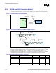
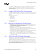
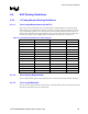
8.3.5. DVOB and DVOC Simulation Method
A model for simulation purposes is shown in Figure 80. The DVO component is a third party-chip.
Figure 80. DVOB and DVOC Simulations Model
GMCH
DVO I/F
DVO
(Device)
DVOB/DVOC
Control, Data
tDVb, tDVa
tDSu, tDh
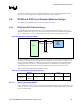
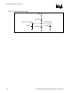
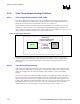
Figure 81. Driver-Receiver Waveforms Relationship Specification
Data1
Data2
Data3
Data4
tDSu tDh
Data1
Data2
Data3
Data4
tDVb
tDVa
Driver
Strobe
Driver
Data
Receiver
Strobe
Receiver
Data
Clock Delay
Data Delay
The setup margin and the hold margin for a particular design depends on the values of the data valid
times and the data setup and hold times on both the driver and the receiver sides. However, note that
available margins are not absolute values. Any skew due to routing and loading differences, any
coupling differences in the parallel traces, and any effects of SSO (ISI, ground bounce, etc.) should be
accounted for in the timing budget as they will reduce the total available margin for the design.
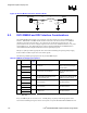
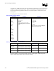
Table 65. Allowable Interconnect Skew Calculation
Component Skew Element Symbol Setup Hold Units
Driver Data Valid before Strobe tDVb 570 ps
Data Valid after Strobe tDVa 770 ps
Interconnect Allowable Skew Vendor specific Vendor specific ps
Receiver Data Setup to Strobe tDSu Vendor specific ps
Data Hold from Strobe tDh Vendor specific ps