
Design Guide
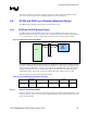

Integrated Graphics Display Port
R
Intel
®
855GM/855GME Chipset Platform Design Guide 173
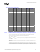
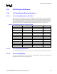
All numbers in this table are from the GMCH specification for DVO interface at 165MHz. For third
party receiver devices, please refer to appropriate third party vendor specifications.
8.4. DVOB and DVOC port Flexible (Modular) Design
The GMCH supports flexible design interfaces described in this section.
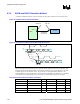
8.4.1. DVOB and DVOC Module Design
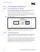
The GMCH supports a DVO module design connected to the GMCH through a generic connector.
Simulation method is the same as in previous section. Lengths L1 and L2 are determined by simulation
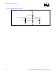
as L1= 4 inches and L2= 2 inches. Refer to Figure 83 for the generic connector parasitic model.
Figure 82. DVO Enabled Simulation Model
DVOB &
DVOC I/F
Generic
Connector
GMCH
Connector
with
DVO
module
tDVb, tDVa
tDSu, tDh
L1 L2
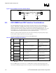
All signals should be routed as striplines (inner layers).All signals in a signal group should be routed on
the same layer. Routing studies have shown that these guidelines can be met. The trace length and trace
spacing requirements must not be violated by any signal. Trace length mismatch for all signals within a
signal group should be as close to ± 100 mils with respect to the strobe clocks as possible to provide
optimal timing margin. Each strobe pair must be separated from other signals by at least 12 mils
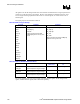
Table 66 shows DVO enabled routing guideline summary.
Table 66. DVO Enabled Routing Guideline Summary
Signal
Maximum
Length
Trace Width Trace Spacing
Length
Mismatch
Notes
DVO Timing
Domain
L1=4 in
L2=2 in
4 mils 8 mils ± 100 mils
8.4.1.1. Generic Connector Model
Figure 83 shows the generic connector model used in simulation for flexible DVO implementation. This
is only for reference. Actual connector may have different parasitic values. Designs using this approach
need to be simulated first.