
Design Guide

AGP Port Design Guidelines
R
178 Intel
®
855GM/855GME Chipset Platform Design Guide
All signals in the 2X/4X timing domain must meet minimum and maximum trace length requirements as
well as trace width and spacing requirements. Because of the multiplexed AGP/DVO interface, there
are trace length matching requirements within each set of 2X/4X signals, as well as between sets of
2X/4X signals.
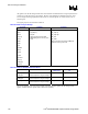
The signal groups are documented in Table 68.
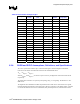
Table 68. AGP 2.0 Signal Groups
1X Signals 2X Signals 4X Signals
CLK (3.3V)
RBF#
WBF#
GST[2:0]
PIPE#
REQ#
GNT#
PAR
FRAME#
IRDY#
TRDY#
STOP#
DEVSEL#
AD[31:0]
C/BE[3:0]#
SBA[7:0]
2X signals include all 1X signals and
AD_STB[1:0]
SB_STB
AD[31:0] signals and associated
C/BE[3:0]# signals are running at 2X
mode.
4X signals include all 1X signals and
AD_STB[1:0]
AD_STB[1:0]#
SB_STB
SB_STB#
AD[31:0] signals and associated C/BE[3:0]#
signals are running at 4X mode.
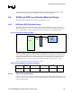
Table 69. AGP 2.0 Data/Strobe Associations
Address/Data Associated Strobe in 1X Associated
Strobe in 2X
Associated Strobes in
4X
AD[15:0] and
C/BE[1:0]#
Strobes are not used in 1X mode. All
data is sampled on rising clock edges.
AD_STB0 AD_STB0, AD_STB0#
AD[31:16] and
C/BE[3:2]#
Strobes are not used in 1X mode. All
data is sampled on rising clock edges.
AD_STB1 AD_STB1, AD_STB1#
SBA[7:0] Strobes are not used in 1X mode. All
data is sampled on rising clock edges.
SB_STB SB_STB, SB_STB#
The routing guidelines for each group of signals (1X timing domain signals, 2X/4X timing domain
signals, and miscellaneous signals) will be addressed separately.