
Design Guide

AGP Port Design Guidelines
R
Intel
®
855GM/855GME Chipset Platform Design Guide 181
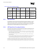
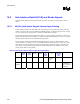
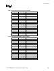
Table 71. Layout Routing Guidelines for AGP 2X/4X Signals
Signal
Maximum
Length (inch)
Trace Space
(mils)
(4 mil traces)
Length
Mismatch
(inch)
Relative To Notes
2X/4X Timing
Domain Set#1
6 8 ± 0.1 AGP_ADSTB0 and
AGP_ADSTB0#
AGP_ADSTB0,
AGP_ADSTB0#
must be the same
length (±10 mils)
2X/4X Timing
Domain Set#2
6 8 ± 0.1 AGP_ADSTB1 and
AGP_ADSTB1#
AGP_ADSTB1,
AGP_ADSTB1#
must be the same
length (±10 mils)
2X/4X Timing
Domain Set#3
6 8 ± 0.1 AGP_SBSTB and
AGP_SBSTB #
AGP_SBSTB,
AGP_SBSTB# must
be the same length
(±10 mils)
9.2.2.3. Trace Length Mismatch Requirements
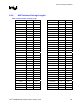
Table 72. AGP 2.0 Data Lengths Relative to Strobe Length
Max Trace Length Trace Spacing Strobe Length Min Trace Length Max Trace Length
< 6 in 1:2 X X – 0.1 in X + 0.1 in
The trace length minimum and maximum (relative to strobe length) should be applied to each set of
2X/4X timing domain signals independently. That is, if AD_STB0 is 5 inches and ADSTB0# is 5.01
inches, then AD[15:0] and C/BE[1:0] must be between 4.91 inches and 5.1 inches. However AD_STB1
and ADSTB1# can be 3.5 inches and 3.51 inches (and therefore AD[31:16] and C/BE#[3:2] must be
between 3.41 inches and 3.6 inches). In addition, all 2X/4X timing domain signals must meet the
maximum trace length requirements.
• All signals should be routed as strip lines (inner layers).
• All signals in a signal group should be routed on the same layer. Routing studies have shown that
these guidelines can be met. The trace length and trace spacing requirements must not be violated
by any signal. Trace length mismatch for all signals within a signal group should be as close to 0
inches as possible to provide optimal timing margin.
The strobe pair must be length matched to less than ± 0.01 inches (that is, a strobe and its compliment
must be the same length within ± 0.01 inches).
Table 73 shows the AGP 2.0 routing summary.