
Design Guide

AGP Port Design Guidelines
R
182 Intel
®
855GM/855GME Chipset Platform Design Guide
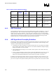
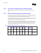
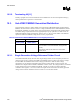
Table 73. AGP 2.0 Routing Guideline Summary
Signal
Maximum
Length
Trace
Spacing
(4 mil
traces)
Length Mismatch Relative To Notes
1X Timing Domain 10 in 4 mils No Requirement N/A None
2X/4X Timing
Domain Set#1
6 in 8 mils ± 0.1 in AD_STB0 and
AD_STB0#
AD_STB0, AD_STB0#
must be the same
length
2X/4X Timing
Domain Set#2
6 in 8 mils ± 0.1 in AD_STB1 and
AD_STB1#
AD_STB1, AD_STB1#
must be the same
length
2X/4X Timing
Domain Set#3
6 in 8 mils ± 0.1 in SB_STB and
SB_STB#
SB_STB, SB_STB#
must be the same
length
9.2.3. AGP Clock Skew
The maximum total AGP clock skew, between the MCH-M and the graphics component, is 1 ns for all
data transfer modes. This 1 ns includes skew and jitter, which originates on the motherboard, add-in
module (if used), and clock synthesizer. Clock skew must be evaluated not only at a single threshold
voltage, but also at all points on the clock edge that falls in the switching range. The 1 ns skew budget is
divided such that the motherboard is allotted 0.9 ns of clock skew (the motherboard designer shall
determine how the 0.9 ns is allocated between the board and the synthesizer).
9.2.4. AGP Signal Noise Decoupling Guidelines
The main focus of these guidelines is to minimize signal integrity problems on the AGP interface of the
Intel 855GME chipset GMCH. The following guidelines are not intended to replace thorough system
validation on Intel 855GME chipset-based products.
• A minimum of six 0.01-µF capacitors are required and must be as close as possible to the GMCH.
These should be placed within 70 mils of the outer row of balls on GMCH for VDDQ decoupling.
Ideally, this should be as close as possible.
• Intel recommends that the designer use a low-ESL ceramic capacitor, such as with a 0603 body-
type X7R dielectric.
• In order to add the decoupling capacitors within 70 mils of the GMCH and/or close to the vias, the
trace spacing may be reduced as the traces go around each capacitor. The narrowing of space
between traces should be minimal and for as short a distance as possible (1.0 inch max.).
In addition to the minimum decoupling capacitors, the designer should place bypass capacitors at vias
that transition the AGP signal from one reference signal plane to another. One extra 0.01-µF capacitor
per 10 vias is required. The capacitor should be placed as close as possible to the center of the via field.