
Design Guide

AGP Port Design Guidelines
R
186 Intel
®
855GM/855GME Chipset Platform Design Guide
9.2.8. AGP VDDQ and VCC
AGP specifies two separate power planes: VCC and VDDQ. VCC is the core power for the graphics
controller. VDDQ is the interface voltage.
9.2.9. VREF Generation for AGP 2.0 (2X and 4X)
9.2.9.1. 1.5-V AGP Interface (2X/4X)
The voltage divider networks consist of AC and DC elements. The reference voltage that should be
supplied to the Vref pins of the graphics controller is ½ * VDDQ. Two 1-kΩ ± 1% resistors can be used
to divide VDDQ down to the necessary voltage level.
The Vref divider network should be placed as close to the AGP interface as is practical to get the benefit
of the common mode power supply effects. However, the trace spacing around the Vref signals must be
a minimum of 25 mils to reduce crosstalk and maintain signal integrity.
9.2.10. AGP Compensation
The Intel 855GME chipset GMCH AGP interface supports resistive buffer compensation. For Printed
Circuit Boards with characteristics impedance of 55 Ω, connect the GRCOMP pin to a 40.2 Ω ± 1%
pull-down resistor (to ground) via a 10-mil wide, very short (≈ 0.5 inches) trace.
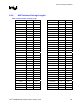
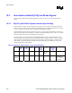
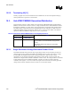
9.2.11. PM_SUS_CLK/AGP_PIPE# Design Consideration
The following design consideration provides the option to support both AGP and DVO devices with one
AGP/ADD Connector. Refer to Figure 86 for more detail.
The GMCH expects PM_SUS_CLK when there is no AGP device. However, when there is an AGP
device this pin functions as AGP_PIPE#. The AGP_TYPEDET# signal is driven high when no AGP
card is detected, allowing DPMS_CLK to be driven by PM_SUS_CLK. In the case where an AGP card
is detected, AGP_TYPE# signal goes high which disconnects PM_SUS_CLK and allows direct connect
of AGP_PIPE# between GMCH and AGP connector.
Figure 86. DPMS Circuit
AGP_TYPEDET#8
AGP_PIPE#_FET
+V12S 17,23,27,37,45
Q6D1
BSS138
3
1
2
Q6D2
BSS138
3
1
2
PM_SUS_CLK
19,37
R6D7 100K
DPMS_CLK
DPMS_CLK 7