
Design Guide

Hub Interface
R
Intel
®
855GM/855GME Chipset Platform Design Guide 187
10. Hub Interface
The GMCH and ICH4-M pin-map assignments have been optimized to simplify the hub interface
routing between these devices. It is recommended that the hub interface signals be routed directly from
the GMCH to the ICH4-M with all signals referenced to VSS. Layer transitions should be kept to a
minimum. If a layer change is required, use only two vias per net and keep all data signals and
associated strobe signals on the same layer.
The hub interface signals are broken into two groups: data signals (HL) and strobe signals (HLSTB).
For the 11-bit hub interface, HL[10:0] are associated with the data signals while HLSTB and HLSTB#
are associated with the strobe signals.
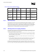
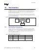
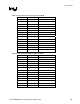
Figure 87. Hub Interface Routing Example
ICH4-M
GMCH
CLK408
CLK66
CLK66
HL[10:0]
HLSTB/HLSTBS
HLSTB#/HLSTBF
10.1. Hub Interface Compensation
This section documents the routing guidelines for the 11-bit hub interface using enhanced (parallel)
termination. This hub interface connects the ICH4-M to the GMCH. The ICH4-M should strap its
HLRCOMP pin to V
CC
=1.5 V, as summarized in Table 77. The 855GM chipset GMCH should strap its
HLRCOMP pin to V
CC
=1.2 V, the 855GME chipset GMCH should strap its HLRCOMP pin to
V
CC
=1.35 V as summarized in Table 77.
The trace impedance must equal 55 Ω ± 15%.
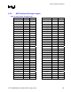
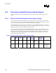
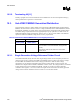
Table 77. Hub Interface RCOMP Resistor Values
Component Trace Impedance HLCOMP Resistor Value HLCOMP Resistor Tied to
ICH4-M 55 Ω ± 15% 48.7 Ω ± 1% Vcc1_5
855GM
GMCH
55 Ω ± 15% 27.4 Ω ± 1% Vcc1_2
855GME
GMCH
55 Ω ± 15% 37.4 Ω ± 1% Vcc1_35