
Design Guide

Hub Interface
R
Intel
®
855GM/855GME Chipset Platform Design Guide 191
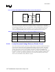
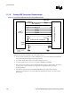
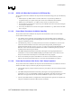
Figure 88. Single VREF/VSWING Voltage Generation Circuit for Hub Interface
ICH4-M
HIREF
R3
R2
C3
C4
VCCHI
C1
C2
HI_VSWING
R1
GMCH
PSWING
HLVREF
C5
C6
The resistor values, R1, R2, and R3 must be rated at 1% tolerance. See Table 82 for recommended
resistor value. The selected resistor values ensure that the reference voltage tolerance is maintained over
the input leakage specification. Two, 0.1-µF capacitors (C1 and C3) should be placed close to the
divider. In addition, the 0.01-µF bypass capacitor (C2, C4, C5, and C6) should be placed within
0.25 inches of HLVREF/VREF pin (for C4 and C6) and HI_VSWING pin (for C2 and C5).
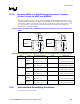
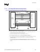
Table 82. Recommended Resistor Values for Single VREF/VSWING Divider Circuit
Recommended Resistor Values VCCHI
Option 1 R1 = 80.6 Ω ± 1% R2 = 51.1 Ω ± 1% R3 = 40.2 Ω ± 1% 1.5 V
Option 2 R1 = 255 Ω ± 1% R2 = 162 Ω ± 1% R3 = 127 Ω ± 1% 1.5 V
Option 3 R1 = 226 Ω ± 1% R2 = 147 Ω ± 1% R3 = 113 Ω ± 1% 1.5 V
C1 and C3 = 0.1 µF (near divider)
C2, C4, C5, C6 = 0.01 µF (near component)
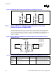
10.3.2. Locally Generated Voltage Reference Divider Circuit
This section describes the option to generate the voltage references separately for GMCH and ICH4-M,
to be used if the routing distance between GMCH and ICH4-M is greater than 4 inches. One voltage
divider circuit is used to generate both HIVREF and HI_VSWING voltage references for ICH4-M.
Another voltage divider circuit is used for GMCH. The reference voltage for both HIVREF and
HI_VSWING must meet the voltage specification in Table 81. The resistor values R1, R2, and R3 must
be rated at 1% tolerance (see Table 82). Normal care needs to be taken to minimize crosstalk to other
signals (< 10-15 mV). If the voltage specifications are not met then individually generated voltage
divider circuit for HIVREF and HI_VSWING is required.