
Design Guide

Hub Interface
R
Intel
®
855GM/855GME Chipset Platform Design Guide 193
10.3.4. Separate GMCH and ICH4-M Voltage Generation / Separate
Divider Circuits for VREF and VSWING
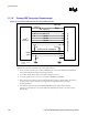
This option allows for tuning the voltage references HIVREF and HI_VSWING individually, for both
ICH4-M and GMCH. The reference voltage for both HIVREF and HI_VSWING must meet the voltage
specification in Table 81. Normal care needs to be taken to minimize crosstalk to other signals (< 10-15
mV). Note that resistor values used for 855GM chipset GMCH and 855GME chipset GMCH are
different since Vcc GMCH is different.
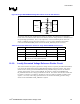
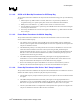
Figure 91. Individual HIVREF and HI_VSWING Voltage Reference Divider Circuits for ICH4-M and
GMCH
V
CC
HI
R4
R5
C1C3
R6
R7
HIVREF
HI_VSWING
C4
C2
ICH4-M
V
CC
GMCH
R8
R9
C1
C3
R10
R11
HLVREF
PSWING
C5
C6
GMCH
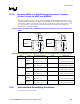
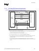
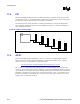
Table 84. Recommended Resistor Values for HIVREF and HI_VSWING Divider Circuits for ICH4-M
Chipset
Component
Signal Recommended Resistor
Values
VCCHI Capacitor value
HIVREF
(350mV)
R4 = 487 Ω ± 1%
R5 = 150
Ω ± 1%,
VCCHI=1.5 V C3 = 0.1 µF (near divider)
C2 = 0.01 µF (near component)
ICH4-M
HI_VSWING
(800mV)
R6 = 130
Ω ± 1%
R7 = 150
Ω ± 1%,
VCCHI=1.5 V C1 = 0.1 µF (near divider)
C4 = 0.01 µF (near component)
HLVREF
(350mV)
R8 = 243 Ω ± 1%
R9 = 100
Ω ± 1%
VCCGMCH=1.2 V C3 = 0.1 µF (near divider)
C6 = 0.01 µF (near component)
855GM
PSWING
(800mV)
R10 = 49.9
Ω ± 1%
R11 = 100
Ω ± 1%
VCCGMCH=1.2 V C1 = 0.1 µF (near divider)
C5 = 0.01 µF (near component)
HLVREF
(350mV)
R8 = 287 Ω ± 1%
R9 = 100
Ω ± 1%
VCCGMCH=1.35 V C3 = 0.1 µF (near divider)
C6 = 0.01 µF (near component)
855GME
PSWING
(800mV)
R10 = 68.1
Ω ± 1%
R11 = 100
Ω ± 1%
VCCGMCH=1.35 V C1 = 0.1 µF (near divider)
C5 = 0.01 µF (near component)
10.4. Hub Interface Decoupling Guidelines
See Section 13.5.5 for more details.