
Design Guide


I/O Subsystem
R
202 Intel
®
855GM/855GME Chipset Platform Design Guide
AC_SDIN1, and AC_SDIN2 may not be driven. If the link is enabled, the assumption can be made that
there is at least one codec.
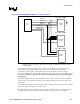
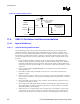
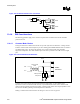
Figure 96. Intel 82801DBM ICH4-M AC’97 – AC_BIT_CLK Topology
AC_BIT_CLK
Intel
®
ICH4
R1
R2
L1 L3 L3 L4
Primary
Codec
L2
C
O
N
N
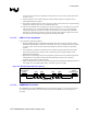
Table 85. AC’97 AC_BIT_CLK Routing Summary
AC’97 Routing Requirements Maximum Trace Length
(inches)
Series Termination
Resistance
AC_BIT_CLK Signal
Length Matching
5 on 5 L1 = (1 to 8) – L3
L2 = 0.1 to 6
L3 = 0.1 to 0.4
L4 = (1 to 6) – L3
R1 = 33
Ω - 47 Ω
R2 = Option 0
Ω resistor
for debugging purposes
N/A
NOTES:
1. Simulations were performed using Analog Device’s* Codec (AD1885) and the Cirrus Logic’s* Codec
(CS4205b). Results showed that if the AD1885 codec was used a 33-
Ω resistor was best for R1 and if the
CS4205b codec was used a 47-
Ω resistor for R1 was best.
2. Bench data shows that a 47-
Ω resistor for R1 is best for the Sigmatel* 9750 codec.
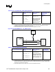
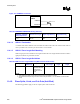
Figure 97. Intel 82801DBM AC’97 – AC_SDOUT/AC_SYNC Topology
AC_SDOUT
Intel
®
ICH4-M
R2
L2
Primary
Codec
L4
L3
L3 L1
R1
C
O
N
N