
Design Guide


I/O Subsystem
R
210 Intel
®
855GM/855GME Chipset Platform Design Guide
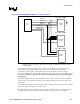
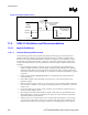
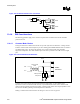
Figure 102. Good Downstream Power Connection
Port1
Port2
G
G
n
n
d
d
V
V
c
c
c
c
4
4
1
1
470pF
Thermister
220uF
G
G
n
n
d
d
V
V
c
c
c
c
4
4
1
1
470pF
5V
5V
Switch
5V Sus
11.4.4. EMI Considerations
The following guidelines apply to the selection and placement of common-mode chokes and ESD
protection devices.
11.4.4.1. Common Mode Chokes
Testing has shown that common-mode chokes can provide required noise attenuation. A design should
include a common-mode choke footprint to provide a stuffing option in the event the choke is needed to
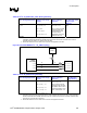
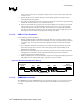
pass EMI testing. Figure 103 shows the schematic of a typical common-mode choke and ESD
suppression components. The choke should be placed as close as possible to the USB connector signal
pins.
Figure 103. Common Mode Choke Schematic
Vcc
USB A
Connector
D+
D-
ESD Supression
Components
Common Mode
Choke
Common mode chokes distort full-speed and high-speed signal quality. As the common mode
impedance increases, the distortion will increase, so you should test the effects of the common mode
choke on full speed and high-speed signal quality. Common mode chokes with a target impedance of 80
Ω to 90 Ω at 100 MHz generally provide adequate noise attenuation.
Finding a common mode choke that meets the designer’s needs is a two-step process.