
Design Guide


I/O Subsystem
R
Intel
®
855GM/855GME Chipset Platform Design Guide 213
micro-controller to perform various functions. For example, the slave write interface can reset or wake a
system, generate SMI# or interrupts, and send a message. The slave read interface can read the system
power state, read the watchdog timer status, and read system status bits.
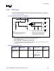
Both the SMBus Host Controller and the SMBus Slave Interface obey the SMBus 1.0 protocol, so the
two interfaces can be externally wire-OR’ed together to allow an external management ASIC (such as
Intel 82562EM 10/100 Mbps Platform LAN Connect) to access targets on the SMBus as well as the
ICH4-M Slave Interface. Additionally, the ICH4-M supports slave functionality, including the Host
Notify protocol, on the SMLink pins. Therefore, in order to be fully compliant with the SMBus 2.0
specification (which requires the Host Notify cycle), the SMLink and SMBus signals must be tied
together externally. This is done by connecting SMLink[0] to SMBCLK and SMLink[1] to SMBDATA.
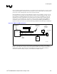
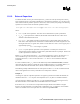
Figure 104. SMBUS 2.0/SMLink Protocol
Intel
®
ICH4
Host Controller and
Slave Interface
SMBus
SMBCLK
SPD Data
Temperature on
Thermal Sensor
Network
Interface Card
on PCI Bus
Microcontroller
Motherboard
LAN
Controller
Wire OR
(optional)
SMLink0
SMLink1
SMLink
SMBDATA
SMbus-SMlink_IF
Intel does not support external access of the ICH4-M’s Integrated LAN Controller via the SMLink
interface. Also, Intel does not support access of the ICH4-M’s SMBus Slave Interface by the ICH4-M’s
SMBus Host Controller. Refer to the Intel
®
82801DBM I/O Controller Hub 4 Mobile (ICH4-M)
Datasheet for full functionality descriptions of the SMLink and SMBus interface.