
Design Guide

I/O Subsystem
R
230 Intel
®
855GM/855GME Chipset Platform Design Guide
Note: Measured trace impedance for layout designs targeting 100 Ω often result in lower actual impedance.
OEMs should verify actual trace impedance and adjust their layout accordingly. If the actual impedance
is consistently low, a target of 105 Ω to 110 Ω should compensate for second order effects.
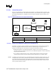
11.9.3.4.2. Distance from Intel 82562ET / 82562ET to Magnetics Module (Distance B)
Distance B should also be designed to be less than one inch between devices. The high-speed nature of
the signals propagating through these traces requires that the distance between these components be
closely observed. In general, any section of traces that is intended for use with high-speed signals should
observe proper termination practices. Proper termination of signals can reduce reflections caused by
impedance mismatches between device and traces. The reflections of a signal may have a high
frequency component that may contribute more EMI than the original signal itself. For this reason, these
traces should be designed to a 100-Ω differential value. These traces should also be symmetric and equal
length within each differential pair.
11.9.3.5. Reducing Circuit Inductance
The following guidelines show how to reduce circuit inductance in both back planes and motherboards.
Traces should be routed over a continuous ground plane with no interruptions. If there are vacant areas
on a ground or power plane, the signal conductors should not cross the vacant area. This increases
inductance and associated radiated noise levels. Noisy logic grounds should be separated from analog
signal grounds to reduce coupling. Noisy logic grounds can sometimes affect sensitive DC subsystems
such as analog to digital conversion, operational amplifiers, etc. All ground vias should be connected to
every ground plane; and similarly, every power via, to all power planes at equal potential. This helps
reduce circuit inductance. Another recommendation is to physically locate grounds to minimize the loop
area between a signal path and its return path. Rise and fall times should be as slow as possible because
signals with fast rise and fall times contain many high frequency harmonics that can radiate
significantly. The most sensitive signal returns closest to the chassis ground should be connected
together. This will result in a smaller loop area and reduce the likelihood of crosstalk. The effect of
different configurations on the amount of crosstalk can be studied using electronics modeling software.
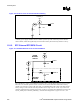
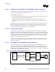
11.9.3.5.1. Terminating Unused Connections
In Ethernet designs, it is common practice to terminate unused connections on the RJ-45 connector and
the magnetics module to ground. Depending on overall shielding and grounding design, this may be
done to the chassis ground, signal ground, or a termination plane. Care must be taken when using
various grounding methods to insure that emission requirements are met. The method most often
implemented is called the “Bob Smith” Termination. In this method, a floating termination plane is cut
out of a power plane layer. This floating plane acts as a plate of a capacitor with an adjacent ground
plane. The signals can be routed through 75-Ω resistors to the plane. Stray energy on unused pins is then
carried to the plane.
11.9.3.5.2. Termination Plane Capacitance
Intel recommends that the termination plane capacitance equal a minimum value of 1500 pF. This helps
reduce the amount of crosstalk on the differential pairs (TDP/TDN and RDP/RDN) from the unused
pairs of the RJ-45. Pads may be placed for an additional capacitance to chassis ground, which may be
required if the termination plane capacitance is not large enough to pass EFT (Electrical Fast Transient)
testing. If a discrete capacitor is used, to meet the EFT requirements it should be rated for at least 1000
Vac.