
Design Guide


I/O Subsystem
R
Intel
®
855GM/855GME Chipset Platform Design Guide 237
at higher frequencies and will degrade the transmit BER performance. Caution should be
exercised if a cap is put in either of these locations. If a cap is used, it should almost certainly be
less than 22 pF. (6 pF to 12 pF values have been used on past designs with reasonably good
success.) These caps are not necessary, unless there is some overshoot in 100 Mbps mode.
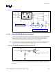
Note: It is important to keep the two traces within a differential pair close
†
to each other. Keeping them close
†
helps to make them more immune to crosstalk and other sources of common-mode noise. This also
means lower emissions (i.e. FCC compliance) from the transmit traces, and better receive BER for the
receive traces.
†
Close should be considered to be less than 0.030 inches between the two traces within a differential
pair. 0.007 inch trace-to-trace spacing is recommended.
11.10. Power Management Interface
11.10.1. SYS_RESET# Usage Model
The System Reset signal (SYS_RESET#) of the ICH4-M can be connected directly to a reset button or
any other equivalent driver in the system where the desired effect is to immediately put the system into
reset. If an Intel Pentium M / Intel Celeron M processor ITP700FLEX debug port is implemented on the
system, it is recommended that the DBR# signal of the ITP interface be connected to SYS_RESET# as
well. If SYS_RESET# is implemented, a weak pull-up resistor pulled-up to the 3.3-V standby rail
(VccSUS3_3) should also be implemented to ensure that no potential floating inputs to SYS_RESET#
cause a system reset. The ICH4-M will debounce signals on this pin (16 ms) and allow the SMBus to go
idle before resetting the system. This delay to allow all outstanding SMBus cycles to complete first and
to prevent a slave device on the SMBus from “hanging” by resetting in the middle of an SMBus cycle.
11.10.2. PWRBTN# Usage Model
The Power Button signal (PWRBTN#) of the ICH4-M can be connected directly to a power button or
any other equivalent driver (e.g. power management controller) where the desired effect is to indicate a
system request to go to a sleep state (if in a normal operating mode) or to cause a wake event (if in a
sleep state already). This signal is internally pulled-up in the ICH4-M to the 3.3-V standby rail
(VccSUS3_3) through a weak pull-up resistor (20 kΩ nominal). The ICH4-M has 16ms of internal
debounce logic on this pin.
11.10.3. Power Well Isolation Control Strap Requirements
The RSMRST# signal of the ICH4 must transition from 20% signal level to 80% signal level and vice-
versa in 50us. Slower transitions may result in excessive droop on the VCCRTC node during Sx-to-G3
power state transitions (removal of AC power). Droop on this node can potentially cause the CMOS to
be cleared or corrupted, the RTC to loose time after several AC power cycles, or the intruder bit might
assert erroneously.