
Design Guide


Platform Clock Routing Guidelines
R
240 Intel
®
855GM/855GME Chipset Platform Design Guide
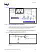
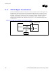
Figure 122 below depicts the system clock subsystem including the clock generator, major platform
components, and all the related clock interconnects.
Figure 122. Clock Distribution Diagram
Platform
Clock Distribution
CK408
CPU
Low Voltage Differential
ICH4-M
CLK33
CLK66
PCI Slot0
PCI Slot1
PCI Slot2
SIO
FWH
PCICLK
CLK33
CLK33
PCICLK
PCICLK
48MHz
PLL
14MHz
PLL
/2
USBCLK
GMCH
100 MHz
Debug
Host clock
DDR Clocks
Differential Pairs
(100/133/167 MHz)
S
O
-
D
I
M
M
S
O
-
D
I
M
M
ITP
CLK14
100MHz
Outputs
CLK66
DOTCLK
SSCCLK
SSC
SSCCLK
DDRCLK s
66MHz
100 MHz
CPU Host
clock
100 MHz
GMCH
Hostclock
12.2. Clock Group Topologies and Routing Constraints
The topology diagrams and routing constraint tables provided on the following pages define the
recommended topology and routing rules for each of the platform level clocks. These topologies and
rules have been simulated and verified to produce the required waveform integrity and timing
characteristics for reliable platform operation.