
Design Guide

Platform Clock Routing Guidelines
R
Intel
®
855GM/855GME Chipset Platform Design Guide 241
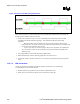
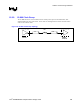
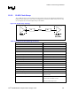
12.2.1. Host Clock Group
The clock synthesizer provides three pairs of 100-MHz differential clock outputs utilizing a 0.7-V
voltage swing. The 100-MHz differential clocks are driven to the processor, the GMCH, and the
processor debug port with the topology shown in the figure below. The host clocks are routed point to
point as closely coupled differential pairs on the motherboard, with dedicated buffers for each of the
three loads. These clocks utilize a Source Shunt Termination scheme as shown below.
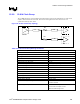
Figure 123. Source Shunt Termination Topology
L1'
L1
Rs
L2
L2'
L3
L3'
L4
L4'
CK408
CPU
GMCH
ITP
Rs
Rt
Rt
The clock driver differential bus output structure is a “Current Mode Current Steering” output which
develops a clock signal by alternately steering a programmable constant current to the external
termination resistors Rt. The resulting amplitude is determined by multiplying IOUT by the value of Rt.
The current IOUT is programmable by a resistor and an internal multiplication factor so the amplitude of
the clock signal can be adjusted for different values of Rt to match impedances or to accommodate
future load requirements.
The recommended termination for the differential bus clock is a “Source Shunt termination.” Parallel Rt
resistors perform a dual function, converting the current output of the clock driver to a voltage and
matching the driver output impedance to the transmission line. The series resistors Rs provide isolation
from the clock driver’s output parasitics, which would otherwise appear in parallel with the termination
resistor Rt.
The recommended value for Rt is a 49.9-Ω ±1% resistor. The tight tolerance is required to minimize
crossing voltage variance. The recommended value for Rs is 33 Ω ± 5%. Simulations have shown that
Rs values above 33 Ω provide no benefit to signal integrity but only degrade the edge rate.
The MULT0 pin (CK408 pin #43) should be pulled-up through a 10 kΩ to VCC – setting the
multiplication factor to 6.
The IREF pin (CK408 pin #42) should be tied to ground through a 475 Ω ± 1 % resistor – making the
IREF 2.32 mA.