
Design Guide
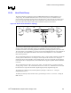
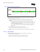

Platform Clock Routing Guidelines
R
242 Intel
®
855GM/855GME Chipset Platform Design Guide
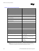
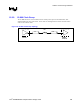
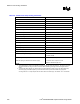
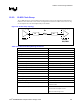
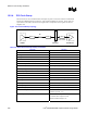
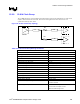
Table 99. Host Clock Group Routing Constraints
Parameter Definition
Class Name HOST_CLK
Class Type Individual Differential Pairs
Topology Differential Source Shunt Terminated
Reference Plane Ground Referenced (contiguous over length)
Single Ended Trace Impedance ( Zo ) 55 Ω +/-15%
Differential Mode Impedance (Zdiff) 100 Ω +/- 15%
Nominal Inner Layer Trace Width 4.0 mils
Nominal Inner Layer Pair Spacing (edge to edge)
(except as allowed below)
7.0 mils
Nominal Outer Layer Trace Width 5.0 mils (pin escapes only)
Nominal Outer Layer Pair Spacing (edge to edge)
(except as allowed below)
5.0 mils
Minimum Spacing to Other Signals 25 mils
Serpentine Spacing 25 mils
Maximum Via Count 5 (per side)
Series Termination Resistor Value 33 Ω +/- 5%
Shunt Termination Resistor Value 49.9 Ω+/- 1%
Trace Length Limits – L1 & L1’ Up to 500mils
Trace Length Limits – L2 & L2’ Up to 200 mils
Trace Length Limits – L3 & L3’ Up to 500 mils
Trace Length Limits – L4 & L4’ 2.0” to 8.0”
Total Length Range– L1 + L2 + L4 2.0” to 8.5”
Length Matching Required Yes (Pin to Pad)
HCLK to HCLK# Length Matching +/- 10 mils (per segment)
+/- 10 mils (overall)
CPU Clock to GMCH Clock Length Matching Match HCLKs (pin to pad) +/- 20 mils
Match L1 segment to +/- 10 mils across all pairs.
(See Section 12.2.1.2.)
CPU Clock to ITP Clock Length Matching Match CPU HCLKs + CPU BPM[3:0]# to ITP HCLKs
+/- 250 mils
(See Section 0)
Breakout Region Exceptions No breakout exceptions allowed.
NOTES:
1. Differential pairs should be routed as a closely coupled side-by-side pair on a single layer over their entire
length.
2. To minimize skew it is recommended that all clocks be routed on a single layer. If clock pairs are to be routed
on multiple layers, the routed length on each layer should be equalized across all clock pairs.