
Design Guide
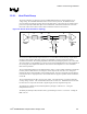
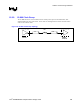
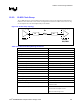
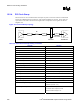

Platform Clock Routing Guidelines
R
246 Intel
®
855GM/855GME Chipset Platform Design Guide
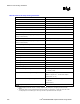
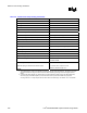
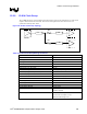
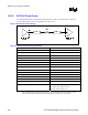
Table 101. CLK66 Clock Group Routing Constraints
Parameter Definition
Class Name CLK66
Class Type Individual Nets
Topology Series Terminated Point to Point
Reference Plane Ground Referenced
Single Ended Trace Impedance ( Zo ) 55 Ω+/-15%
Nominal Inner Layer Trace Width 4.0 mils
Nominal Outer Layer Trace Width 5.0 mils (pin escapes only)
Minimum Spacing (see exceptions below) 20 mils
Serpentine Spacing 20 mils
Maximum Via Count 4
Series Termination Resistor Value 33 Ω+/- 5 %
Trace Length Limits – L1 Up to 500mils (breakout segment)
Trace Length Limits – L2 4.0” to 8.5”
Total Length Range – L1 + L2 4.0” to 9.0”
Minimum Length Requirements CLK66 < HCLK + X.X"
Length Matching Required Yes (Pin to Pin)
Clock to Clock Length Matching +/- 100 mils
CLK66 to CLK66
Breakout Region Exceptions
(Reduced spacing for GMCH & ICH breakout region)
5 mil trace with 5 mil space on outers
4 mil trace with 4 mil space in inners
Maximum breakout length is 0.3”
NOTES:
1. The overall length of CLK66 is considered the reference length for CLK33 and PCICLK. The length of this clock
should be set within the range and then used as the basis for defining the length of all other length matched
clocks
2. A trace length offset (depends on CK408 vendor clock skew) between CLK66 going to the GMCH (GCLKIN)
and HCLK going to the GMCH (BCLK) is recommended in order to prevent the CLK66 rising edge from
occurring within the +/- 350ps keepout area on either side of the HCLK edge. See Section 12.2.1.3 for details.