
Design Guide

Platform Clock Routing Guidelines
R
Intel
®
855GM/855GME Chipset Platform Design Guide 249
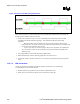
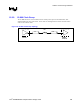
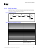
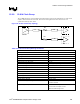
12.2.5. CLK14 Clock Group
The 14-MHz clocks are series terminated and routed point to point on the motherboard. A single clock
output is shared between the two loads. These clocks are length tuned to each other but are not
synchronous with any other clocks.
Figure 128. CLK14 Clock Group Topology
L1
Rs
CK408
ICH4-M
L2A
SIO
L2B
Rs
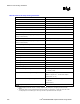
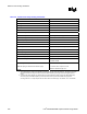
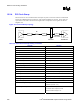
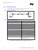
Table 104. CLK14 Clock Group Routing Constraints
Parameter Definition
Class Name CLK14
Class Type Individual Nets
Topology Dual Series Terminated Point to Point
Reference Plane Ground Referenced
Single Ended Trace Impedance ( Zo ) 55 Ω+/-15%
Nominal Inner Layer Trace Width 4.0 mils
Nominal Outer Layer Trace Width 5.0 mils (pin escapes only)
Minimum Spacing (see exceptions below) 20 mils
Serpentine Spacing 20 mils
Maximum Via Count 4 (per driver/receiver path)
Series Termination Resistor Value 33 Ω+/- 5 %
Trace Length Limits – L1 Up to 500 mils
Trace Length Limits – L2A, L2B 2.0” to 8.5”
Total Length Range – L1 + L2A & L1 + L2B 2.0” to 9.0”
Length Matching Required Yes (Pin to Pin)
Clock to Clock Length Matching +/- 500 mils
CLK14A to CLK14B
Breakout Region Exceptions
5 mil trace with 5 mil space on outers
4 mil trace with 4 mil space in inners
Maximum breakout length is 0.3”