
Design Guide


Platform Clock Routing Guidelines
R
Intel
®
855GM/855GME Chipset Platform Design Guide 251
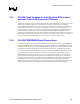
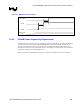
12.2.7. SSCCLK Clock Group
The 48/66-MHz SSCCLK operates independently and is not length tuned to any other clock. This clock
employs a spread-spectrum device in its path to reduce EMI. The overall clock path is divided into two
segments as shown in Figure 130, with each segment series terminated and routed point to point.
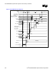
Figure 130. SSCCLK Clock Topology
L1
Rs
CK408 GMCH
L2 SSC
L3
Rs
L4
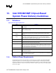
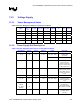
Table 106. SSCCLK Clock Routing Constraints
Parameter Definition
Class Name SSCCLK
Class Type Individual Net
Topology Series Terminated Point to Point
Reference Plane Ground Referenced
Single Ended Trace Impedance ( Zo ) 55 Ω+/-15%
Nominal Inner Layer Trace Width 4.0 mils
Nominal Outer Layer Trace Width 5.0 mils (pin escapes only)
Minimum Spacing (see exceptions below) 20 mils
Maximum Via Count 4 (per driver/receiver path)
Series Termination Resistor Value 33 Ω+/- 5 %
Trace Length Limits – L1 Up to 500 mils
Trace Length Limits – L2 1.0” to 4.0”
Trace Length Limits – L3 Up to 500 mils
Trace Length Limits – L4 1.0” to 7.0”
Total Length Range – L1 + L2 + L3 + L4 3.0” to 8.5”
Length Matching Required No
Breakout Exceptions
5 mil trace with 5 mil space on outers
4 mil trace with 4 mil space in inners
Maximum breakout length is 0.3”