
Design Guide


Intel 855GM/GME Chipset Based System Power Delivery Guidelines
R
256 Intel
®
855GM/855GME Chipset Platform Design Guide
The solutions given in this document are only examples. There are many power distribution methods
that achieve similar results. It is critical, when deviating from these examples, to consider the effect of
the change.
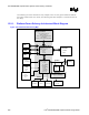
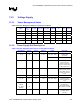
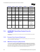
13.2.1. Platform Power Delivery Architectural Block Diagram
Figure 132. Platform Power Delivery Map
LVDS
CRT
PCI Bus
Docking
400MHz BPSB
Intel® Pentium® M Processor /
Dothan Processor
VCC_CORE = IMVP-IV
VCCP = IMVP-IV
855GM/GME GMCH
VCC-GMCH = 1.35V / 1.2V
+V1.5S
+V 2.5
+V3.3S
DVO
ICH4-M
+V1.5S
+V1.5Always
+V3.3Always
+V3.3S
+V3.3LAN
+V5Always
Hub Interface 1.5
FWH
+V3.3S
+V2.5
+V1.25S
CardBus LAN
+V3.3 +V3.3
AC97
USB
+V3.3
+V5Always
ATA 66/100
IDE
+V3.3S
+V5S
SIO
KBC
SMC
+V3.3Always
+V3.3Always+V3.3S
+V3.3
+V3.3Always
+V5
VCCP = IMVP-IV
200/266/333
MHz DDR
+V1.5LAN
+VCC_RTC
VCCA =+V1.8S (Intel® Pentium®
M Processor)
VCCP = IMVP-IV
Intel® PRO/ Wireless
network connection
Mini PCI
LPC I/F
VCCA =+V1.5S (Dothan Processor)