
Design Guide

Intel 855GM/GME Chipset Based System Power Delivery Guidelines
R
258 Intel
®
855GM/855GME Chipset Platform Design Guide
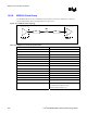
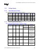
Signal Names Voltage
(V)
Current
(A)
Tolerance Enable Description
+V3ALWAYS 3.3 0.4 +/- 5% +VDC_ON ICH4-M Resume,
SMC/KBC, AC’97
+V3 3.3 0.9 +/- 5% SLP_S5# - HIGH ICH4-M LAN I/O,
AC’97, RS232
+V3S 3.3 7.0 +/- 5% SLP_S3# - HIGH GMCH GPIO, ICH4-M
I/O, CK-408, FWH,
SIO,PCI
+V5 5 9.0 +/- 5% SLP_S5# - HIGH AC’97,
+V5S 5 1.0 +/- 5% SLP_S3# - HIGH ICH4-M VREF,
MSE/KBD, FDD, IDE,
PCI
+V5ALWAYS 5 3.0 +/- 5% +VDC ICH4-M VREFSUS,
USB Supply
+V12S 12 0.2 +/- 5% SLP_S3# - HIGH PCI, IDE
+VCC_CORE 0.844 -
1.356
32 ±1.5%
(static)
VID Intel Pentium M / Intel
Celeron M processor
core voltage by IMVP-
IV VR
± 10 mV (ripple &
transient)
+VCCP 1.05 2.4 +/- 5% VR_ON Intel Pentium M / Intel
Celeron M processor
I/O voltage by IMVP-IV
VR
NOTE: GMCH VREF, DDR memory VREF, DDR termination, and GMCH TXLVDS can be turned off during S3.
However, for some DDR memory devices may require a valid reference voltage during S3.
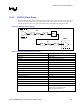
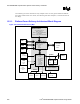
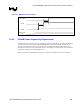
13.4. 855GM/GME Chipset Based System Power-Up
Sequence
The following sections describe the power-up timing sequence for Intel 855GM/GME chipset GMCH
based platforms.
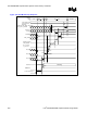
13.4.1. Processor Power Sequence Requirement
Contact your Intel Field Representative for details on the Intel Pentium M processor or Intel Celeron M
processor with IMVP-IV voltage regulator..
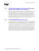
13.4.2. GMCH Power Sequencing Requirements
All GMCH power rails should be stable before PWROK is asserted. The power rails can be brought up
in any order desired. However, good design practice would have all GMCH power rails come up as
close in time as practical, with the core voltage (1.2 V for 855GM / 1.35 V for 855GME) coming up
first. RSTIN#, which brings GMCH out of reset, should be deasserted only after PWROK has been
active for 1 ms. Once GMCH is out of reset, it will deassert CPURST# within 1 ms.