
Design Guide


System Overview
R
26 Intel
®
855GM/855GME Chipset Platform Design Guide
2.2. Intel 855GM Platform Component Features
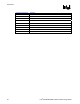
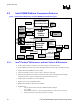
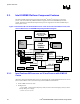
Figure 1. Intel Pentium M Processor and Intel 855GM Chipset Block Diagram
Intel® Pentium® M
Processor or Intel
Celeron® M Processor
LPC I/F
AC'97 2.2/2.3
PCI Bus
Hub Interface 1.5
Intel®
82801DBM
421 BGA
(ICH4-M)
Intel® 855GM
GMCH
732 Micro-
FCBGA
FWH
DVI
Device
DVOB & DVOC
1.5 V
400 MHz BPSB
200/266 MHz
DDR
KBC
SIO
Audio Codec
Modem Codec
ATA100 IDE (2)
USB2.0/1.1 (6)
CK-408
Cardbus
LAN
Moon 2
PCI Docking
Intel® PRO/
Wireless
Network
Connection
Mini-PCI
IMVP-IV
VR
LVDS
CRT
2.2.1. Intel
®
Pentium
®
M Processor and Intel Celeron M Processor
• On-die primary 32-kbyte, instruction cache and 32-kbyte, write-back data cache
• On-die 1-MB second level cache; On-die 512-kB second level cache (Intel Celeron M Processor)
• Supports Streaming SIMD Extensions 2 (SSE2)
• Advanced Gunning Transceiver Logic (AGTL+) bus driver technology
• Enhanced Intel SpeedStep technology to enable real-time dynamic switching between multiple
voltage and frequency points (not supported by Intel Celeron M processor)
• Supports host bus dynamic bus inversion (DINV)
• Dynamic power down of Data Bus buffers
• BPRI# control to Disable Address/Control buffers
• Package/Power
478-pin, Micro-FCPGA and 479-ball Micro-FCBGA packages
VCC-CORE:
Intel Pentium M processor: 1.484 V (highest frequency mode) to 0.844 V (lowest
frequency mode); 0.748 V (Deeper Sleep) core voltage