
Design Guide

Intel 855GM/GME Chipset Based System Power Delivery Guidelines
R
Intel
®
855GM/855GME Chipset Platform Design Guide 263
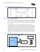
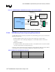
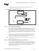
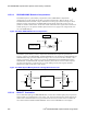
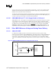
Figure 137. V5REFSUS With +V3ALWAYS and +V5S or +V5 Connection Option
Note: D1 and D2 are BAT54 or Equivalent Schottky Diodes
+V5S or +V5
+V3ALWAYS
USB D+
V5REF_SUS2
USB D+
USB D-
ICH4
-
M
USB D-
USB Power (5V)
GND
Customer specific or
Intel recommended
USB interface
circuits
D2
0.1uF
Customer specific or
Intel recommended
USB power circuit
D1
USB D+
V5REF_SUS1
USB D+
USB D-
ICH4
-
M
USB D-
USB Power (5V)
GND
Customer specific or
Intel recommended
USB interface
circuits
D2
0.1uF
Customer specific or
Intel recommended
USB power circuit
D1
13.4.4. DDR Memory Power Sequencing Requirements
No DDR-SDRAM power sequencing requirements are specified during power up or power down if the
following criteria are met:
• VDD and VDDQ to memory devices are driven from a single power converter output.
• VTT is limited to 1.44 V (reflecting VDDQ(max)/2 + 50 mV VREF variation + 40 mV VTT
variation)
• VREF tracks VDDQ/2
• A minimum resistance of 42 Ω (22 Ω series resistor + 22 Ω parallel resistor ± 5% tolerance) limits
the input current from the VTT supply into any pin.
If the above criteria cannot be met by the system design, then the following Table 112 must be adhered
to during power up. Refer to Intel
®
DDR 200 JEDEC Spec Addendum for more details.
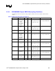
Table 112. DDR Power-Up Initialization Sequence
Voltage Description Sequencing Voltage Relationship to Avoid Latch-up
VDDQ After or with VDD < VDD + 0.3 V
VTT After or with VDDQ < VDDQ + 0.3 V
VREF After or with VDDQ < VDQ + 0.3 V