
Design Guide

Intel 855GM/GME Chipset Based System Power Delivery Guidelines
R
264 Intel
®
855GM/855GME Chipset Platform Design Guide
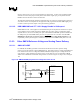
13.5. Intel 855GM/GME Chipset Based System Power
Delivery Guidelines
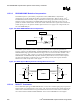
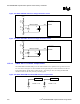
Each component is capable of generating large current swings when switching between logic high and
logic low. This condition could cause the component voltage rails to drop below specified limits. To
avoid this type of situation, ensure that the appropriate amount of bulk capacitance is added in parallel to
the voltage input pins. Intel recommends that the developer use the amount of decoupling capacitors
specified in this document to ensure the component maintains stable supply voltages. The capacitors
should be placed as close to the package as possible. Rotate caps that set over power planes so that the
loop inductance is minimized (see Figure 138). The basic theory for minimizing loop inductance is to
consider which voltage is on Layer 2 (power or ground) and spin the decoupling cap with the opposite
voltage towards the BGA (Ball Grid Array). This greatly minimizes the total loop inductance. Intel
recommends that for prototype board designs, the designer should include pads for extra power plane
decoupling caps.
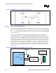
Figure 138. Example for Minimizing Loop Inductance
Layer 1
Layer 2
Layer 3
Layer 4
GND
GND
4.5 mils nominal
48 mils nominal
BGA
BALL
BGA
BALL
BGA
Sbt t
PAD
Trace
connecting
Pad to Via
VIA
GND
Ball
PWR
Ball
Copper
Plane
Under BGA
Decoupling
Cap
PWR
Current Flow to Decoupling Cap