
Design Guide

Intel 855GM/GME Chipset Based System Power Delivery Guidelines
R
Intel
®
855GM/855GME Chipset Platform Design Guide 269
tolerance and VTT can vary more easily depending on signal states. A solid 1.25V termination island
should be used to for this purpose and be placed on the surface signal layer, just beyond the last SO-
DIMM connector and must be at least 50 mils wide.
The Data and Command signals should be terminated using one resistor per signal. Resistor packs and ±
5% tolerant resistors are acceptable for this application. Only signals from the same DDR signal group
can share a resistor pack. See Chapter 6 for system memory guidelines.
13.5.2.5. DDR SMRCOMP and VTT 1.25-V Supply Disable in S3/Suspend
SMRCOMP and VTT 1.25V supplies can be disabled during the S3 suspend state to further save power
on the platform. This is possible because the GMCH does not require resistive compensation during
suspend. However, the 2.5-V VCCSM power pins of the GMCH, the SMVREF pin of the GMCH, and
the VDD power pins of the DDR memory devices are required
to be on in S3 state. Note that some
DDR memory devices may or may not require a valid reference voltage during suspend. It is the
responsibility of the system designer to ensure that requirements of the DDR memory devices are met.
13.5.3. Other GMCH Reference Voltage and Analog Power Delivery
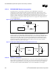
13.5.3.1. GMCH GTLVREF
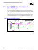
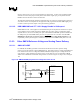
For GMCH, the GTLREF generation circuit has been broken down into three separate voltage
references; host data reference voltage (HDVREF[2:0]), host address reference voltage (HAVREF) and
host common clock reference voltage (HCCVREF). Maximum length from pin to voltage divider for
each reference voltage should be less than 0.5 inches. 10 mil wide traces are recommended. GMCH
VREF can be maintained as individual voltage dividers as shown in Figure 142, Figure 143, and Figure
144.
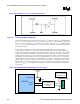
Figure 142. GMCH HDVREF[2:0] Reference Voltage Generation Circuit
R1
49.9
1
%
R2
100
1
%
C1
1u
F
+VCCP
K21
J21
J1
7
GMCH
HDVREF0
HDVREF1
HDVREF2
0.1uF
GMCH_HDVREF
C2