
Design Guide
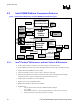
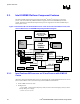

System Overview
R
Intel
®
855GM/855GME Chipset Platform Design Guide 27
Intel Celeron M processor: 1.356 V (Standard Voltage core version), 1.004 V (Ultra-
Low Voltage core version)
VCCA (1.8 V):
VCCP (1.05 V)
2.2.2. Intel
®
855GM Chipset Graphics Memory Controller Hub (GMCH)
2.2.2.1. Intel Pentium M Processor and Intel Celeron M Processor FSB Support
• Optimized for Intel Pentium M/Intel Celeron M processor in 478-pin Micro-FCPGA package
• AGTL+ bus driver technology with integrated GTL termination resistors (gated AGTL+ receivers
for reduced power)
• Supports 32-bit AGTL+ bus addressing (no support for 36-bit address extension)
• Supports Uni-processor (UP) systems
• 400-MHz, source-synchronous PSB
• 2X Address, 4X data
• 12 deep In-Order queue
2.2.2.2. Integrated System Memory DRAM Controller
• Supports up to two double-sided SO-DIMMs (four rows populated) with unbuffered
PC1600/PC2100 DDR-SDRAM (with or without ECC)
• Supports 64-Mb, 128-Mb, 256-Mb, and 512-Mb technologies for x8 and x16 width devices
• Maximum of 1 GB of system memory with 512-Mb technology devices; maximum of 2 GB of
system memory with high-density 512Mb technology devices
• Supports 200-MHz and 266-MHz DDR devices
• 64-bit data interface (72-bit with ECC)
• Supports up to 16 simultaneous open pages
• Support for SO-DIMM serial presence detect (SPD) scheme via SMBus interface
• S3 power management support via self refresh mode using CKE
2.2.2.3. Internal Graphics Controller
• Graphics Core Frequency
Display / Render frequency up to 200 MHz
• 3D Graphics Engine
3D Setup and Render Engine
Zone Rendering
High quality performance Texture Engine
• Analog Display Support
350-MHz integrated 24-bit RAMDAC
Hardware color cursor support