
Design Guide

Intel 855GM/GME Chipset Based System Power Delivery Guidelines
R
270 Intel
®
855GM/855GME Chipset Platform Design Guide
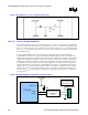
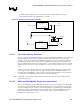
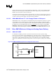
Figure 143. GMCH HAVREF Reference Voltage Generation Circuit
R1
49.9
1
%
R2
100
1
%
C1
1u
F
+VCCP
Y22
GMCH
HAVREF
C3
0.1uF
GMCH_HAVREF
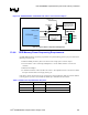
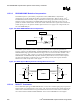
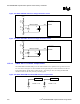
Figure 144. GMCH HCCVREF Reference Voltage Generation Circuit
R1
49.9
1
%
R2
100
1
%
C1
1u
F
+VCCP
Y28
GMCH
HCCVREF
C
3
0.1uF
GMCH_HCCVREF
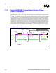
13.5.3.2. GMCH AGTL+ I/O Buffer Compensation
The HXRCOMP and HYRCOMP pins of the GMCH should each be pulled-down to ground with a 27.4
Ω ± 1% resistor. See Figure 145. The maximum trace length from pin to resistor should be less than 0.5
inches and should be 18-mil wide to achieve the Zo = 27.4 Ω target. Also, the routing for HRCOMP
should be at least 25 mils away from any switching signal.
Figure 145. GMCH HXRCOMP and HYRCOMP Resistive Compensation
27.4
Ω
+/- 1%
HXRCOMP
27.4
Ω
+/- 1%
HYRCOMP