
Design Guide

Intel 855GM/GME Chipset Based System Power Delivery Guidelines
R
Intel
®
855GM/855GME Chipset Platform Design Guide 271
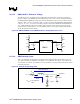
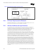
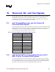
13.5.3.3. GMCH AGTL+ Reference Voltage
The GMCH’s AGTL+ I/O buffer resistive compensation mechanism also requires the generation of
reference voltages to the HXSWING and HYSWING pins with a value of 1/3*VCCP. Implementations
for HXSWING and HYSWING voltage generation are illustrated in Figure 146. Two resistive dividers
with R1a = R1b = 301 Ω ± 1% and R2a = R2b = 150 Ω ± 1% generate the HXSWING and HYSWING
voltages. C1a = C1b = 0.1 µF act as decoupling capacitors and connect HXSWING and HYSWING to
VCC_CORE. HSWING components should be placed within 0.5 inches of their respective pins and
connected with a 15-mil wide trace. To avoid coupling with any other signals, maintain a minimum of
25 mils of separation to other signals.
Figure 146. GMCH HXSWING and HYSWING Reference Voltage Generation Circuit
R1a
301
R2a
150
C1a
+VCCP
GMCH
HXSWING
HXSWING HYSWING
R1b
301
R2b
150
C1b
+VCCP
HYSWING
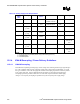
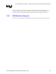
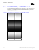
13.5.3.4. GMCH Analog Power
Table 114 summarizes the eight analog circuits that require filtered supplies on the GMCH. They are:
VCCASM, VCCQSM, VCCAHPLL, VCCADPLLA, VCCADPLLB, VCCADAC, VCCAGPLL, and
VCCALVDS. VCCADAC, VCCAGPLL, and VCCALVDS do not require an RLC filter but do require
decoupling capacitors.
Figure 147. Example Analog Supply Filter
Low Pass Filtering
Noise
L
C
BULK
C
HIGH
V
CC
Filtered V
CC
*R
DAMP
*R
DAMP
*R
DAMP
is not required for
filters