
Design Guide

System Overview
R
28 Intel
®
855GM/855GME Chipset Platform Design Guide
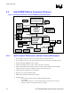
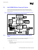
Accompanying I2C and DDC channels provided through multiplexed interface
Dual independent pipe for dual independent display
Simultaneous display: same images and native display timings on each display device
• Digital Video Out Port (DVOB and DVOC) support
DVOB & DVOC with 165-MHz dot clock support for each 12-bit interface
Compliant with DVI Specification 1.5
• Dedicated LFP (local flat panel) support
Single or dual channel LVDS panel support up to UXGA panel resolution with frequency range
from 25 MHz to 112 MHz per channel
SSC support of 0.5%, 1.0%, and 2.5% center and down spread with external SSC clock
Supports data format of 18 bpp
LCD panel power sequencing compliant with SPWG timing specification
Compliant with ANSI/TIA/EIA –644-1995 spec
Integrated PWM interface for LCD backlight inverter control
Bi-linear Panel fitting
2.2.2.4. Package/Power
• 732-pin Micro-FCBGA (37.5 mm x 37.5 mm)
• VTTLF, VTTHF (1.05 V)
• VCC, VCCASM, VCCHL, VCCAHPLL, VCCAGPLL, VCCADPLLA, VCCADPLLB (1.2 V)
• VCCADAC, VCCDVO, VCCDLVDS, VCCALVDS, (1.5 V)
• VCCSM, VCCQSM, VCCTXLVDS (2.5 V)
• VCCGPIO (3.3 V)
2.2.3. Intel
®
82801DBM I/O Controller Hub 4-Mobile (ICH4-M)
• Upstream Accelerated Hub Architecture interface for access to the GMCH
• PCI 2.2 interface (6 PCI Request/Grant Pairs)
• Bus Master IDE controller (supports Ultra ATA 100/66/33)
• USB 1.1 and USB 2.0 Host Controllers
• I/O APIC
• SMBus 2.0 Controller
• FWH Interface
• LPC Interface
• AC’97 2.2 / 2.3 Interface
• Alert-On-LAN*
• IRQ Controller
• Package/Power
421-pin, BGA package (31 mm x 31 mm)
VCC1_5 (1.5 V main logic voltage), VCC3_3 (3.3 V main I/O voltage)